9.3.18.3 IOBUF_UTX
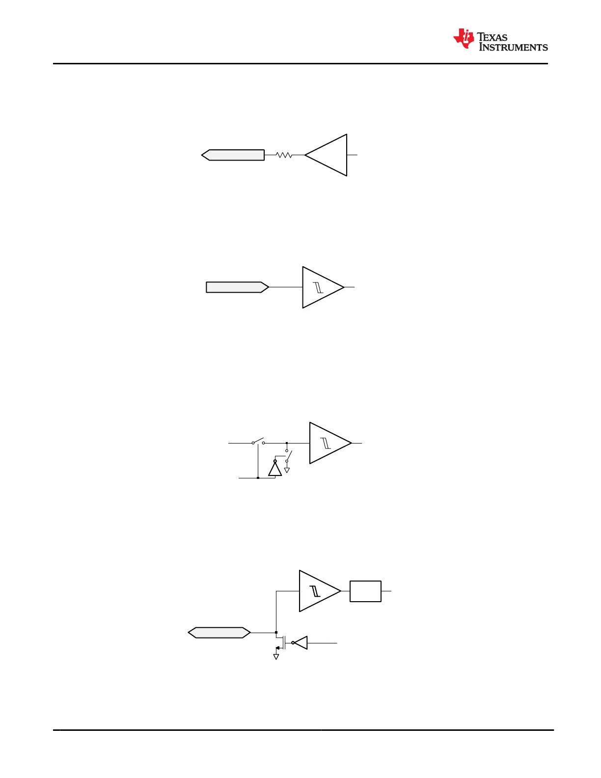
The push-pull output driver is shown in Figure 9-48. The output buffer has a UARTTX_RO source resistance.
The supply voltage to the system side buffer is configurable to be LDO_3V3 by default or VDDIO. This is not
shown in Figure 9-48. The supply voltage to the port side buffers remains LDO_3V3.
CMOS
Output
UART_TXout
UARTTX_RO
UART_TX
Figure 9-48. IOBUF_UTX Output Buffer
9.3.18.4 IOBUF_URX
The input buffer is shown in Figure 9-49. The supply voltage to the system side buffer is configurable to be
LDO_3V3 by default or VDDIO. This is not shown in Figure 9-49. The supply voltage to the port side buffers
remains LDO_3V3.
Figure 9-49. IOBUF_URX Input
9.3.18.5 IOBUF_PORT
The input buffer is shown in Figure 9-50. This input buffer is connected to the intermediate nodes between
the 1
st
stage switch and the 2
nd
stage switch for each port output (C_SBU1/2, C_USB_TP/N, C_USB_BN/P).
The input buffer is enabled via firmware when monitoring digital signals and disabled when an analog signal
is desired. See theFigure 9-36 section for more detail on the pullup and pulldown resistors of the intermediate
node.
Figure 9-50. IOBUF_PORT Input Buffer
9.3.18.6 IOBUF_I2C
The I
2
C I/O driver is shown in Figure 9-51. This I/O consists of an open-drain output and an input comparator
with deglitching. The supply voltage to this buffer is configurable to be LDO_3V3 by default or VDDIO. This is not
shown in Figure 9-51. Parameters for the I
2
C clock and data I/Os are found in Section 7.20.
I2C_IRQnZ
I2C_DO
I2C_DI
50 ns
Deglitch
Figure 9-51. IOBUF_I2C I/O
9.3.18.7 IOBUF_GPIOHSPI
Figure 9-52 shows the I/O buffers for the SPI interface.
TPS65982
SLVSD02E – MARCH 2015 – REVISED AUGUST 2021
www.ti.com
68 Submit Document Feedback
Copyright © 2021 Texas Instruments Incorporated
Product Folder Links: TPS65982