20 V source power contract to another device. When the DC Barrel Jack is disconnected the TPS65982 will exit
any 20 V source power contract and re-negotiate a power contract. When the DC Barrel Jack is connected the
TPS65982 will send updated source capabilities and re-negotiate a power contract if needed.
The PFET enable will be controlled by the DC barrel jack detect comparator depicted in Figure 10-5. This will
allow the system to power up from dead battery through the barrel jack as well as the Type-C ports. Figure
10-7 shows the flow between changing from DC barrel jack charging and USB-PD charging. The example uses
back-to-back PFETs for disabling and enabling the power path for the DC Barrel Jack. It is important to use
PFETs that are rated above the specified parameters to ensure robustness of the system. The DC Barrel Jack
voltage in this design is assumed to be 20 V at 5 A, so the PFETs are recommended to be rated at a minimum of
30 V and 10 A of current.
The TPS65982 in this design also provides the GPIO control for the PFET gate drive that passes the DC Barrel
Jack Voltage to the system. Figure 10-7 shows the flow between changing from DC Barrel Jack charging and
Type-C PD charging.
10.2.2.2.4 Primary TPS65982 Flash Controller and Secondary Port
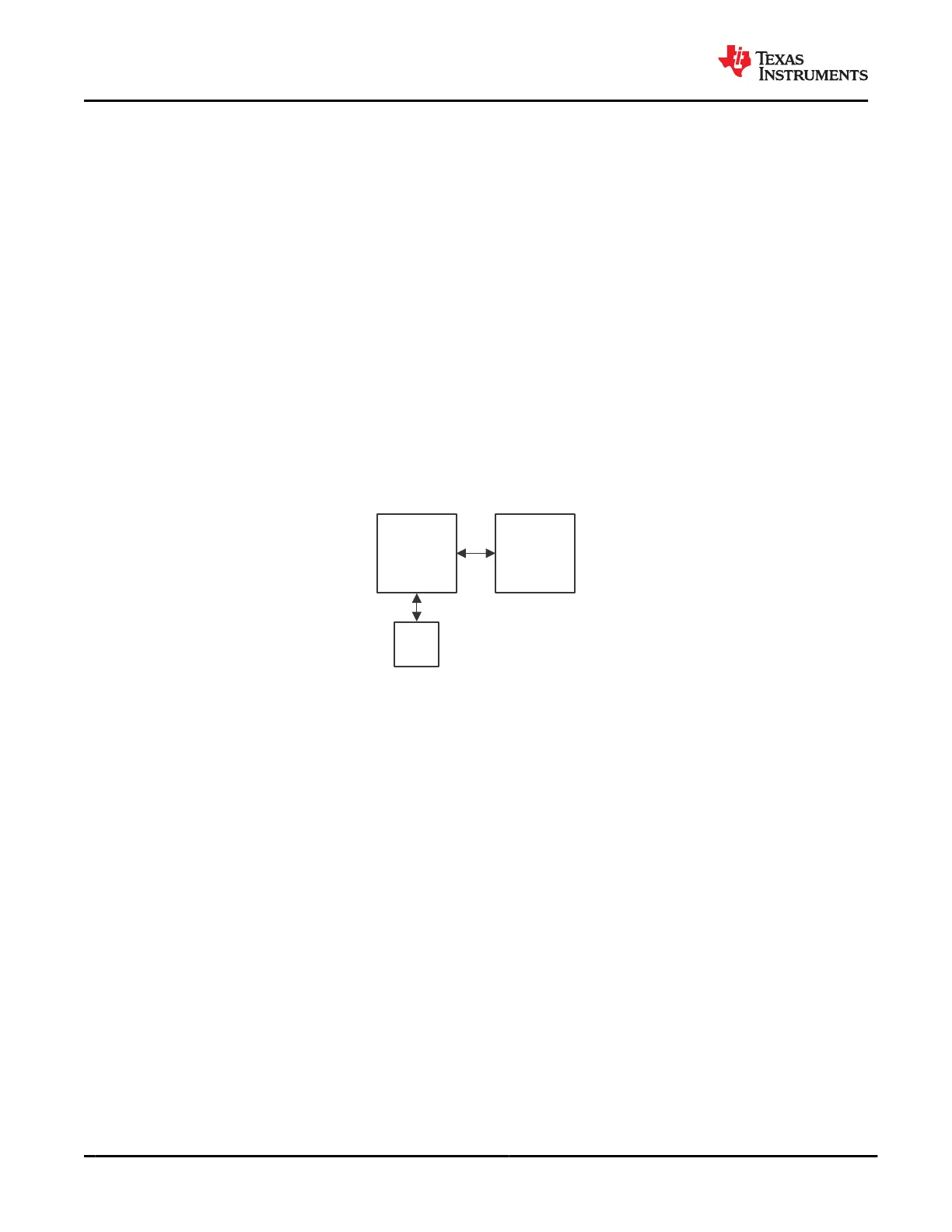
A single flash can be used for two TPS65982’s in a system where the primary TPS65982 is connected to the
flash and the seoncdary TPS65982 is connected to the primary through UART. UART data is used to pass the
firmware from the primary TPS65982 to the secondary TPS65982 in the system. Figure 10-6 shows a simplified
block diagram of how a primary and secondary TPS65982 are connected using a single flash. The primary
TPS65982 must have its I2C_ADDR pin tied to GND with a 0Ω to denote it as the primary TPS65982.
TPS65982
(Primary)
TPS65982
(Secondary)
SPI
Flash
SPI
UART
Figure 10-6. Primary and Secondary TPS65982 Sharing a Single Flash
10.2.2.2.5 TPS65982 Dead Battery Support Primary and Secondary Port
The TP65982 supports dead battery functionality to be able to power up from the Type-C port. This design
supports dead battery using the PP_EXT path, where RPD_G1/2 and CC1/2 are connected respectively,
and BUSPOWERZ is connected to GND to path 5 V VBUS into the system through the PP_EXT path. The
TPS65982 will soft-start the PP_EXT (or PP_HV) path to comply with USB2.0 inrush current requirements.
To enable PD functionality the TPS65982 must boot the application firmware from the flash. For the primary
TPS65982, once VBUS is detected at 5 V it will automatically start to load the application firmware from the
flash. The TPS65982 will then be able communicate over PD and establish a power contract at the required 20
V. Figure 10-8 shows the boot up sequence of the primary TPS65982.
When the TPS65982 that is not connected to the flash is connected in dead battery it will pass the 5 V from
VBUS in to the battery charger where the battery would be able to generate the needed System 3.3 V rail to both
of the TPS65982s. Once the primary TPS65982 has a valid 3.3 V supply (VBUS = 0 V on Primary TPS65982) it
will load the application firmware from the flash and pass it to the secondary TPS65982 that is connected. Once
the secondary TPS65982 has loaded the application firmware over UART it will be able to negotiate a 20-V
power contract. Figure 10-9 shows the dead battery sequence of the secondary TPS65982.
10.2.2.2.6 Debugging Methods
The TPS65982 has methods of debugging a Type-C and PD system. In addition to the resistances
recommended in the I
2
C (I2C), Debug Control (DEBUG_CTL), and Single-Wire De-bugger (SWD Resistors
section, additional series resistors are used for debugging. The two I
2
C channels allow a designer to check
the system state through the Host Interface Specification. By attaching 0-Ω series resistors between the I
2
C
master and the TPS65982 and additionally adding 0-Ω series resistors between the TPS65982 and test points,
TPS65982
SLVSD02E – MARCH 2015 – REVISED AUGUST 2021
www.ti.com
88 Submit Document Feedback
Copyright © 2021 Texas Instruments Incorporated
Product Folder Links: TPS65982