1
Introduction
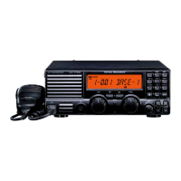
This manual provides technical information necessary for servicing the VX-4000L VHF Low-band FM Transceiver.
Servicing this equipment requires expertise in handling surface-mount chip components. Attempts by non-qualified
persons to service this equipment may result in permanent damage not covered by the warranty, and may be illegal in
some countries.
Two PCB layout diagrams are provided for each double-sided circuit board in the Transceiver. Each side of is referred
to by the type of the majority of components installed on that side (“leaded” or “chip-only”). In most cases one side has
only chip components, and the other has either a mixture of both chip and leaded components (trimmers, coils, electrolyt-
ic capacitors, ICs, etc.), or leaded components only.
While we believe the technical information in this manual to be correct, VERTEX STANDARD assumes no liability
for damage that may occur as a result of typographical or other errors that may be present. Your cooperation in pointing
out any inconsistencies in the technical information would be appreciated.
©2004 VERTEX STANDARD CO., LTD. EC005L90A
Service Manual
VX-4000L
VHF Low-band FM Transceiver
Operating Manual Reprint......................... 1-1
Cloning ..................................................................
2-1
Specifications................................................ 2-2
Exploded View & Miscellaneous Parts.... 3-1
Block Diagram .............................................. 3-2
Interconnection Diagram............................ 3-4
Circuit Description ..................................... 4-1
Alignment...................................................... 5-1
Contents
Board Unit (
Schematics, Layouts & Parts
)
MAIN Unit ........................................................... 6A-1
DISPLAY Unit ...................................................... 6B-1
KEY Unit ...............................................................6C-1
VR Unit ................................................................. 6D-1
MIC CONN Unit................................................. 6D-2
Optional Board Unit (
Schematics, Layouts & Parts
)
F2D-8 2-Tone Decode Unit ................................ 7A-1
F5D-14 5-Tone Unit ............................................. 7B-1
FVP-25 Encryption / DTMF Pager Unit ............7C-1
VTP-50 VX-Trunk Unit ...................................... 7D-1
POWER
VERTEX STANDARD CO., LTD.
4-8-8 Nakameguro, Meguro-Ku, Tokyo 153-8644, Japan
VERTEX STANDARD
US Headquarters
10900 Walker Street, Cypress, CA 90630, U.S.A.
YAESU EUROPE B.V.
P.O. Box 75525, 1118 ZN Schiphol, The Netherlands
YAESU UK LTD.
Unit 12, Sun Valley Business Park, Winnall Close
Winchester, Hampshire, SO23 0LB, U.K.
VERTEX STANDARD HK LTD.
Unit 5, 20/F., Seaview Centre, 139-141 Hoi Bun Road,
Kwun Tong, Kowloon, Hong Kong