EasyManua.ls Logo

Vertex Standard VX-424A Series User Manual

Vertex Standard VX-424A Series
50 pages
To Next Page IconTo Next Page
Page #1 background imageLoading...
Page #1 background image
1
Introduction
This manual provides technical information necessary for ser-
vicing the VX-424A (LTR
®
) Series FM Transceiver.
Servicing this equipment requires expertise in handling surface-
mount chip components. Attempts by non-qualified persons to
service this equipment may result in permanent damage not cov-
ered by the warranty, and may be illegal in some countries.
Two PCB layout diagrams are provided for each double-sided
circuit board in the transceiver. Each side of is referred to by the
type of the majority of components installed on that side (“lead-
ed” or “chip-only”). In most cases one side has only chip com-
ponents, and the other has either a mixture of both chip and lead-
ed components (trimmers, coils, electrolytic capacitors, ICs, etc.),
or leaded components only.
While we believe the technical information in this manual to be
correct, VERTEX STANDARD assumes no liability for dam-
age that may occur as a result of typographical or other errors
that may be present. Your cooperation in pointing out any in-
consistencies in the technical information would be appreciated.
LTR
®
is a registered trademark of E.F Johnson Company.
©
2009 VERTEX STANDARD CO., LTD. EC071N95C
Service Manual
VX-424A (LTR
®
) Series
VHF FM Transceiver
Specifications ..........................................................2
Exploded View & Miscellaneous Parts ..............3
Block Diagram .........................................................5
Circuit Description ................................................7
Alignment ................................................................9
Contents
Board Unit (
Schematics, Layouts & Parts
)
MAIN-2 Unit ............................................................ 25
DUMMY Unit .......................................................... 47
Optional Units (
Schematics, Layouts & Parts
)
FVP-25 Encryption / DTMF Pager Unit .............. 48
VERTEX STANDARD CO., LTD.
4-8-8 Nakameguro, Meguro-Ku, Tokyo 153-8644, Japan
VERTEX STANDARD
US Headquarters
10900 Walker Street, Cypress, CA 90630, U.S.A.
YAESU UK LTD.
Unit 12, Sun Valley Business Park, Winnall Close
Winchester, Hampshire, SO23 0LB, U.K.
VERTEX STANDARD HK LTD.
Unit 5, 20/F., Seaview Centre, 139-141 Hoi Bun Road,
Kwun Tong, Kowloon, Hong Kong
VERTEX STANDARD
(
AUSTRALIA
)
PTY., LTD.
Normanby Business Park, Unit 14/45 Normanby Road
Notting Hill 3168, Victoria, Australia
16 key Version 4 key Version
Important Note
This transceiver was assembled using Pb (lead) free solder, based on the RoHS specification.
Only lead-free solder (Alloy Composition: Sn-3.0Ag-0.5Cu) should be used for repairs performed on this appara-
tus. The solder stated above utilizes the alloy composition required for compliance with the lead-free specification,
and any solder with the above alloy composition may be used.
Question and Answer IconNeed help?

Do you have a question about the Vertex Standard VX-424A Series and is the answer not in the manual?

Vertex Standard VX-424A Series Specifications

General IconGeneral
BrandVertex Standard
ModelVX-424A Series
CategoryTransceiver
LanguageEnglish

Summary

Introduction to Service Manual

Servicing Requirements and Risks

Expertise needed for surface-mount components; risks for unauthorized servicing and potential legal issues.

PCB Layout Diagram Explanation

Explains diagrams for double-sided boards, referencing "leaded" or "chip-only" sides.

Important Solder Information

Lead-Free Solder Specification

Transceiver uses lead-free solder; repairs must use lead-free solder for compliance.

Technical Specifications

General Operating Parameters

Covers frequency, channels, voltage, temperature, dimensions, and weight.

Receiver and Transmitter Performance

Details sensitivity, selectivity, output power, modulation, and noise figures.

Exploded View and Parts Identification

Front Case and Keypad Components

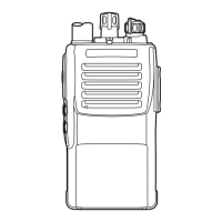
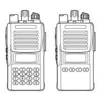
Details parts for the front case, including light guide, speaker, and keypad assembly.

Main Unit and Rear Case Components

Lists parts for the main unit, rear case, and terminal plates.

Battery Pack and Belt Clip Assembly

Shows the battery pack and belt clip assembly.

Block Diagram of Radio Unit

MAIN-2 Unit Signal Flow

Illustrates the signal paths and components within the MAIN-2 unit.

Transmit and Receive Signal Paths

Shows signal flow for transmit and receive functions, including VCO and PLL.

Circuit Description

Receive Signal Path Details

Details the RF signal path from antenna to audio output, including filters and mixers.

Squelch Control Circuitry

Explains how the squelch operates based on noise detection and microprocessor control.

Transmit Signal Path Details

Describes the audio signal path from microphone to RF output, including modulation and PLL.

Circuit Description - Advanced Functions

Transmit Power Control and Inhibit

Explains automatic transmit power control and transmitter inhibit logic.

PLL Frequency Synthesizer Operation

Details the PLL circuitry for receive and transmit frequencies, including VCO and phase locking.

Push-To-Talk Activation

Explains how the PTT switch activates transmission and disables the receiver.

Alignment Procedure Introduction

Required Test Equipment and Software

Lists required test equipment and software for alignment.

Alignment Preparation and Precautions

Outlines precautions like temperature control, dummy loads, and warming up equipment.

CT-42 Connection for Programming

Instructions for connecting the CT-42 plug for programming, including removing the cap.

Initial Alignment Steps

Test Equipment Setup and Channel Data

Describes test equipment setup and recommends programming channel data before alignment.

PLL VCV Alignment Procedure

Details steps for adjusting the PLL VCV using TP2045, L2036, and L2038.

Alignment Tool Operation

Software Installation and Setup

Instructions for installing the VX-424A Programming Software on a PC.

Reference Frequency Alignment

Steps to align the reference frequency using the software and a slide bar.

Transmitter Output Power Alignment

High and Low Power Output Adjustment

Steps to adjust high (5.0 W) and low (1.0 W) power outputs using the software's slide bar.

Deviation Alignment

Maximum Deviation (Wide and Narrow Bands)

Adjusts maximum deviation for wide and narrow bands using a 2 kHz tone.

CTCSS Deviation Alignment

CTCSS Deviation (Wide and Narrow Bands)

Adjusts CTCSS deviation for wide and narrow bands using a CTCSS test tone.

Modulation Balance Alignment

Modulation Balance (Wide and Narrow Bands)

Adjusts modulation balance for wide and narrow bands, without microphone input.

DCS Deviation Alignment

DCS Deviation (Wide and Narrow Bands)

Adjusts DCS deviation for wide and narrow bands using a DCS test tone.

LTR Deviation Alignment

LTR Deviation (Wide and Narrow Bands)

Adjusts LTR deviation for wide and narrow bands using an LTR test tone.

Tone and Standard Deviation Alignment

Sequential Tone and STD Deviation Alignment

Adjusts sequential tone deviation and standard deviation (MIC Gain).

Squelch and RX Tune Alignment

RX Tune (Sensitivity) and Tight Noise Squelch Alignment

Tunes receiver sensitivity and aligns the tight noise squelch level.

Squelch Threshold and RSSI Alignment

Threshold Noise Squelch and Tight Noise Squelch RSSI Alignment

Aligns threshold noise squelch level and tight noise squelch RSSI.

Squelch RSSI and Threshold Alignment

Tight Noise Squelch RSSI (Wide) and Threshold Noise Squelch (Narrow)

Aligns tight noise squelch RSSI (wide) and threshold noise squelch (narrow).

TX Save RSSI Alignment

TX Save RSSI (Wide and Narrow Bands)

Aligns TX Save RSSI for wide and narrow bands with specified output levels.

Alignment Procedure Completion

Finalizing Alignment and Radio Power Off

Completes the alignment routine by exiting the software and turning off the radio.

MAIN-2 Unit Circuit Diagram

MAIN-2 Unit Parts Layout

Parts Layout - Side A

Illustrates the component placement on the MAIN-2 unit, Side A.

Parts Layout - Side B

Illustrates the component placement on the MAIN-2 unit, Side B.

MAIN-2 Unit Parts List

Capacitors and Diodes Components

Lists capacitors (C2002-C2181) and diodes (D2001-D2050) with their specifications.

Resistors and Inductors Components

Lists resistors (R2002-R2345) and inductors (L2001-L2038) with their specifications.

DUMMY Unit Circuit Diagram

DUMMY Unit Parts List

FVP-25 Encryption / DTMF Pager Unit Circuit Diagram

FVP-25 Encryption / DTMF Pager Unit Parts List

Related product manuals