EMB-9670/9673 Series
46 EMB-9670/9673 Series User’s Manual
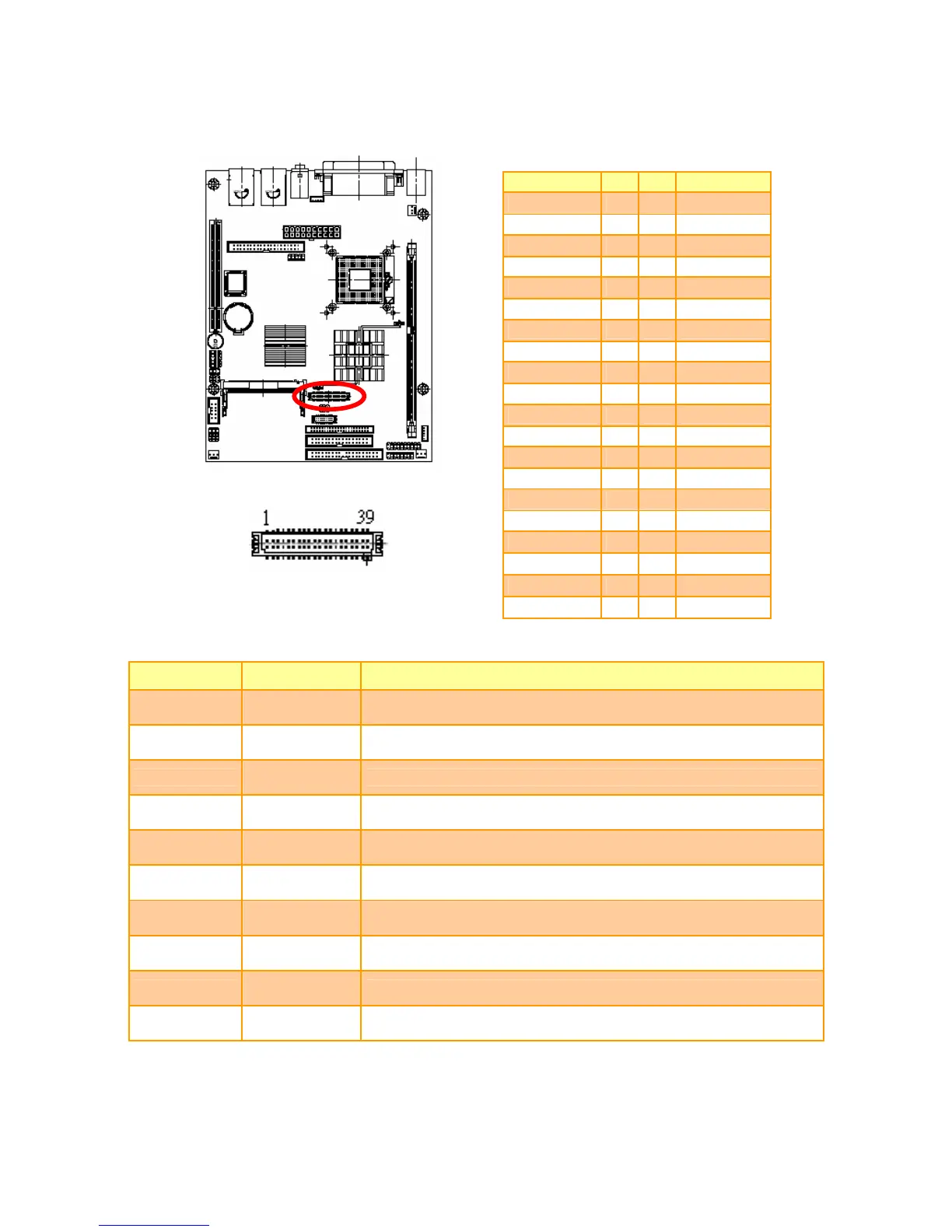
2.3.25 LVDS Connector (JLVDS)
Signal PIN PIN Signal
+5V 2 1 +3.3V
+5V 4 3 +3.3V
SPDATA 6 5 SPCLK
GND 8 7 GND
YA0P 10 9 YA1P
YA0M 12 11 YA1M
GND 14 13 GND
YA2P 16 15 YA3P
YA2M 18 17 YA3M
GND 20 19 GND
YB0P 22 21 YB1P
YB0M 24 23 YB1M
GND 26 25 GND
YB2P 28 27 YB3P
YB2M 30 29 YB3M
GND 32 31 GNDG
CLK1P 34 33 CLK2P
CLK1M 36 35 CLK2M
GND 38 37 GND
Reserved 40 39 Reserved
2.3.26 Signal Description – LVDS Connector (JLVDS)
Signal Type Signal Description
SPDATA
I/O
CMOS
Panel DDC Data: This signal is used as the DDC data signal between
the LFP and the GMCH.
SPCLK
I/O
CMOS
Panel DDC Clock: This signal is used as the DDC clock signal
between the LFP and the GMCH.
YA[0:3]P
O
LVDS
Channel A differential data pair 3:0 output (true): 245-800 MHz.
YA[0:3]M
O
LVDS
Channel A differential data pair 3:0 output (compliment): 245--800
MHz
YB[0:3]P
O
LVDS
Channel B differential data pair 3:0 output (true): 245-800 MHz.
YB[0:3]M
O
LVDS
Channel B differential data pair 3:0 output (compliment): 245- 800
MHz.
CLK1P
O
LVDS
Channel A differential clock pair output (true): 245-800 MHz
CLK1M
O
LVDS
Channel A differential clock pair output (compliment): 245- 800
MHz.
CLK2P
O
LVDS
Channel B differential clock pair output (true): 245-800 MHz
CLK2M
O
LVDS
Channel B differential clock pair output (compliment): 245- 800
MHz.
 Loading...