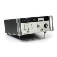
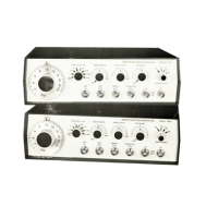
Model
2001
CIRCUIT DESCRIPTION
put cable to turn on a pin diode, located in the M19H module,
which couples the band 1 RF output into the RF output
system.
ELECTRONIC ATTENUATOR
Ahead of the first RF amplifier is an electronic attenuator
consisting of PIN diodes,
CRI, CR2, and CR3 which pro-
vides variable RF conductance proportional to the positive
current supplied through the switching transistor
07.
LEVELER OUTPUT (PIN 6)
The leveler amplifier (09,
Q10, and Q11) provides leveling
of the RF output for Bands 1, 2 and 3 by supplying a posi-
tive current to the electronic attenuator system for each
band as directed by the band switching voltages (B-1, B-2,
and
8-3) which turn on the correct switching transistor for
that band (in the
MlOH module or the M19H module).
A positively increasing output voltage from the leveler am-
plifier will increase the RF output level. RF blanking
is
effected by a positive input voltage (pin 4) to switching
transistor Q8 which causes the leveler output (pin 6) to go
negative during sweep retrace time shutting off the elec-
tronic attenuator.
LEVELER INPUTS (Pin 5 and Pin
7)
A monitor diode, located external to the MIOH, provides
a negative DC voltage related to the RF output level present
in the output system. The output system and monitor diode
is located in the
M19H module or in an external monitor
circuit. This negative voltage is connected to one input of
the operational amplifier, consisting of
Q9, 010, and 01
1.
Since an increasingly negative voltage at the input will re-
duce the positive current supplied to each electronic
atten-
uator, the RF output level is held constant, by negative
feedback, at a level determined by a reference voltage. This
reference voltage varies under control of the LEVEL PRO-
GRAM input voltage at pin 7 of the
MIOH module. The
magnitude of this negativevoltage is determined by the MAX
pot which
sets
the maximum RF level when the program
voltage
is
maximum (-18 volts). The MIN pot provides a
small negative reference voltage which determines the mini-
mum RF level when the level program voltage at pin 7 is
zero.
4.8
SWEEP
OSCILLATOR, BANDS
2
&
3
(MODULE M19H)
This module contains two separate sweep oscillators, each
with itsvoltagevariable attenuator and the necessary switch-
ing circuitry to connect either band
I,
band
2,
or band 3 to
the common monitor and RF output connector.
Band 1 is connected to the RF output circuit by PIN diode
CR9. The control current for switching this diode is con-
tained in the
MIOH module.
Band 2 oscillator, consisting of
06 and its associated cir-
cuitry, is a common base oscillator varactor-tuned by CR2,
CR3, CR4 and CR5. Biasing of the varactor diodes is pro-
vided by
Q1 and 02. Q3 is a switching transistor which
disconnects the bias voltage from the varactors when the
unit is operated on band
1
or band
3.
The B -voltage for
the oscillator
is
modulated by the blanking signal, from pin
4, in transistor stages Q4 and Q5. This modulation causes
the oscillator to be cut off during the sweep retrace period,
thereby providing a zero RF output level during the retrace
time. The RF signal
is
coupled from the oscillator, by L9,
to a voltage variable attenuator consisting of CR6, CR7
and CR8. This attenuator
is
part of the closed loop leveling
system consisting of the monitor diode
CR20, the leveler
amplifier, (located in the
MIOH module) and the voltage
variable attenuator. The operation of this circuit maintains
a constant amplitude RF signal at the monitor point and
also allows adjustment of this signal over a
20dB
range.
Since the effective impedance at the monitor point is zero
ohms, R46 establishes the output impedance at approxi-
mately 50 ohms.
Band 3 oscillator is almost identical to band 2. The os-
cillator tank inductance has been decreased and the oscilla-
tor transistor, 014, is operated at a slightly higher current.
The varactor bias is provided by
09 and 010 and the B-
blanking is provided by
Q11 and Q12. Current during the
sweep retrace time is not completely removed but
is
steered
by
01
3
through CR 12. This current will not cause oscilla-
tion since L15 has been by-passed. It does, however, pro-
vide better frequency stability in the oscillator. The RF
signal is coupled from the oscillator, by L20, through the
voltage variable attenuator consisting of CR 17, CR18 and
CR 19 and to the RF output.
Q7
and Q8 help provide the proper bias to the shunt diodes
in the voltage variable attenuators, in order to maintain a
constant load for the oscillator, thus minimizing the fre-
quency pulling effects of the attenuator.
Model 2001
put
cable
to
turn
on
a pin
diode,
located in
the
M 19H
module,
which
couples
the
band
1 R F
output
into
the
R F
output
system.
ELECTRONIC
ATTENUATOR
Ahead
of
the
first RF amplifier
is
an
electronic
attenuator
consisting
of
PIN diodes, CR 1,
CR2,
and
CR3
which pro-
vides variable R F
conductance
proportional
to
the
positive
current
supplied
through
the
switching
transistor
07.
LEVELER
OUTPUT
(PIN 6)
The
leveler amplifier
(09,
010,
and
011)
provides leveling
of
the
R F
output
for
Bands 1, 2 and 3 by
su
pplying a posi-
tive
current
to
the
electronic
attenuator
system
for each
band
as
directed
by
the
band switching voltages (B-1, B-2,
and
B-3)
which
turn
on
the
correct
switching
transistor
for
that
band
(in
the
MlOH
module
or
the
M19H module).
A positively increasing
output
voltage from
the
leveler am-
plifier will increase
the
RF
output
level. RF blanking
is
effected
by a positive
input
voltage (pin
4)
to
switching
transistor
08
which causes
the
leveler
output
(pin 6)
to
go
negative
during
sweep retrace time
shutting
off
the
elec-
tronic
attenuator.
LEVELER
INPUTS (pin 5
and
Pin
7)
A
monitor
diode,
located external
to
the
Ml0H,
provides
a negative
DC
voltage related
to
the
RF
output
level
present
in
the
output
system.
The
output
system and
monitor
diode
is
located
in
the
M19H
module
or
in
an
external
monitor
circuit. Th
is
negative voltage
is
connected
to
one
input
of
the
operational
amplifier, consisting
of
09,010,
and
011.
Since an increasingly negative voltage
at
the
input
will
re-
duce
the
positive
current
supplied
to
each
electronic
atten-
uator,
the
R F
output
level
is
held
constant,
by negative
feedback,
at
a level
determined
by a reference Voltage. This
reference voltage varies
under
control
of
the
LEVEL
PRO-
GRAM
input
voltage
at
pin 7
of
the
Ml0H
module.
The
magnitude
of
this
negative voltage
is
determined
by
the
MAX
pot
which
sets
the
maximum
R F level
when
the
program
voltage
is
maximum
(-18 volts).
The
MIN
pot
provides a
small negative reference voltage which
determines
the
mini-
mum
RF level
when
the
level program voltage
at
pin 7
is
zero.
CIRCUIT
DESCRIPTION
4.8
SWEEP
OSCILLATOR, BANDS 2 & 3
(MODULE
M19H)
This
module
contains
two
separate
sweep oscillators, each
with
its voltage variable
attenuator
and
the
necessary switch-
ing
circuitry
to
connect
either
band
1, band 2,
or
band
3
to
the
common
monitor
and RF
output
connector.
Band 1
is
connected
to
the
R F
output
circuit
by
PI
N
diode
CR9.
The
control
current
for
switching
this
diode
is
con-
tained
in
the
Ml0H
module.
Band 2 oscillator, consisting
of
06
and its associated cir-
cuitry,
is
a
common
base oscillator
varactor-tuned
by
CR2,
CR3,
CR4
and CR5. Biasing
of
the
varactor
diodes
is
pro-
vided by
01
and
02.
03
is
a switching
transistor
which
disconnects
the
bias voltage from
the
varactors
when
the
unit
is
operated
on
band
1
or
band
3.
The
B -voltage for
the
oscillator
is
modulated
by
the
blanking signal,
from
pin
4,
in
transistor stages
04
and
05.
This
modulation
causes
the
oscillator
to
be
cut
off
during
the
sweep
retrace
period,
thereby
providing a
zero
R F
output
level
during
the
retrace
time.
The
RF signal
is
coupled
from
the
oscillator, by L9,
to
a voltage variable
attenuator
consisting
of
CR6,
CR7
and
CR8.
This
attenuator
is
part
of
the
closed
loop
leveling
system consisting
of
the
monitor
diode
CR20,
the
leveler
amplifier, (located
in
the
Ml0H
module) and
the
voltage
variable
attenuator.
The
operation
of
this
circuit
maintains
a
constant
amplitude
R F signal
at
the
monitor
point
and
also allows
adjustment
of
this signal over a 20dB range.
Since
the
effective
impedance
at
the
monitor
point
is
zero
ohms,
R46
establishes
the
output
impedance
at
approxi-
mately
50
ohms.
Band 3 oscillator
is
almost
identical
to
band 2.
The
os-
cillator
tank
inductance
has been decreased and
the
oscilla-
tor
transistor,
014,
is
operated
at
a slightly higher
current.
The
varactor
bias
is
provided by
09
and
010
and
the
8-
blanking
is
provided by
011
and
012.
Currentduringthe
sweep retrace
time
is
not
completely
removed
but
is
steered
by
013
through
CR 12. This
current
will
not
cause
oscilla-
tion
si
nce L
15
has been by-passed. I t does, however, pro-
vide
better
frequency
stability
in
the
oscillator.
The
RF
signal
is
coupled
from
the
oscillator, by L20,
through
the
voltage variable
attenuator
consisting
of
CR 17, CR
18
and
CR
19 and
to
the
R F
output.
07
and
08
help provide
the
proper
bias
to
the
shunt
diodes
in
the
voltage variable
attenuators,
in
order
to
maintain
a
constant
load for
the
oscillator,
thus
minimizing
the
fre-
quency pulling effects of
the
attenuator.
4-7
 Loading...