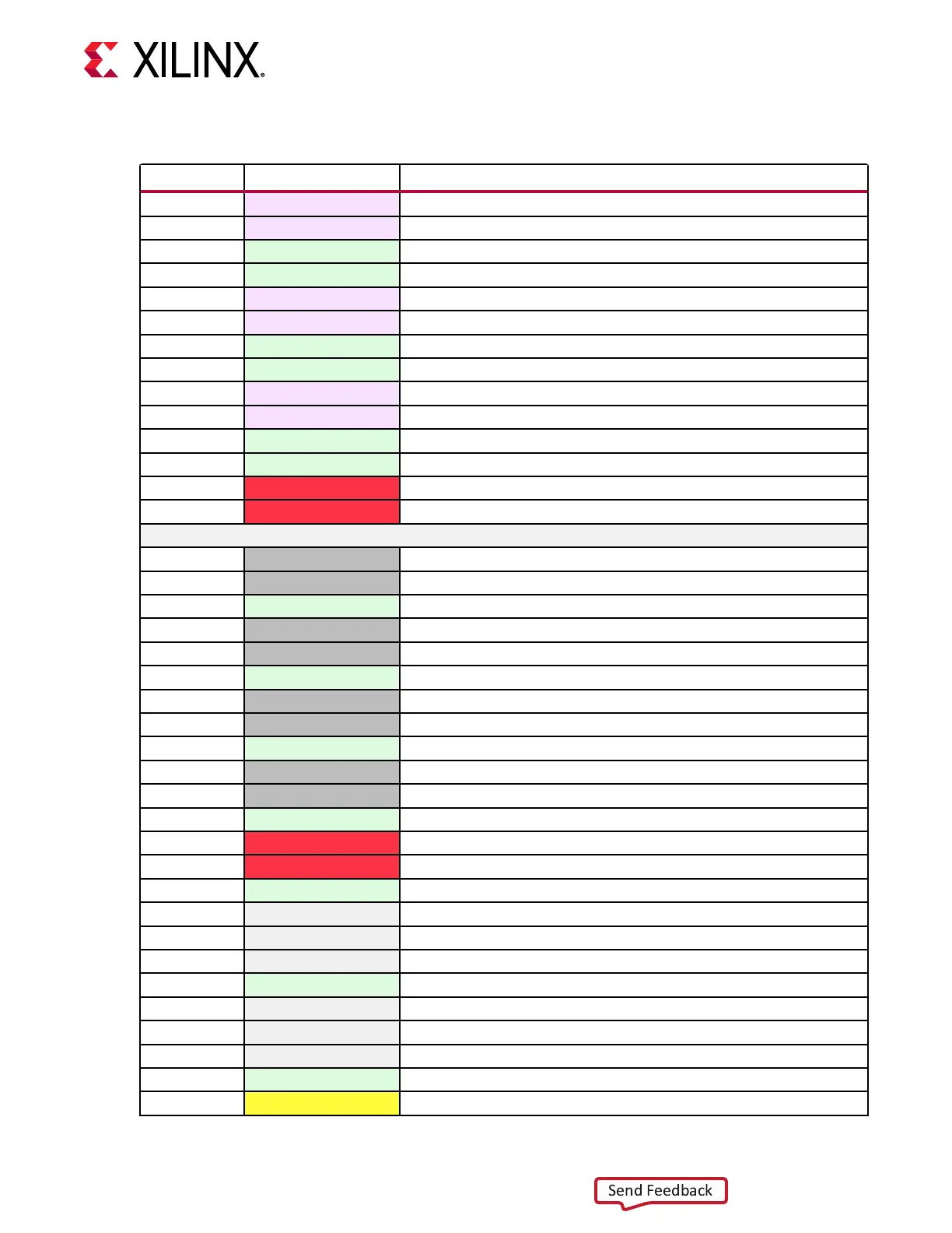
Table 4: SOM240_1 Signal Pins (cont'd)
Pin Number Signal Name Signal Description
A47 GTR_DP1_M2C_P PS-GTR lane 1 TX
A48 GTR_DP1_M2C_N PS-GTR lane 1 TX
A49 GND Ground
A50 GND Ground
A51 GTR_REFCLK3_C2M_P PS-GTR REFCLK3 input
A52 GTR_REFCLK3_C2M_N PS-GTR REFCLK3 input
A53 GND Ground
A54 GND Ground
A55 GTR_DP0_C2M_P PS-GTR lane 0 RX
A56 GTR_DP0_C2M_N PS-GTR lane 0 RX
A57 GND Ground
A58 GND Ground
A59 VCC_SOM SOM main supply voltage, +5V
A60 VCC_SOM SOM main supply voltage, +5V
Connector Row B
B1 HPA05_CC_P HPIO clock-capable pin on bank 66
B2 HPA05_CC_N HPIO clock-capable pin on bank 66
B3 GND Ground
B4 HPA04_P HPIO on bank 66
B5 HPA04_N HPIO on bank 66
B6 GND Ground
B7 HPA07_P HPIO on bank 66
B8 HPA07_N HPIO on bank 66
B9 GND Ground
B10 HPA11_P HPIO on bank 66
B11 HPA11_N HPIO on bank 66
B12 GND Ground
B13 VCCO_HDA HDA I/O voltage rail, 1.2V to 3.3V
B14 VCCO_HDA HDA I/O voltage rail, 1.2V to 3.3V
B15 GND Ground
B16 HDA03 HDIO on bank 45
B17 HDA04 HDIO on bank 45
B18 HDA05 HDIO on bank 45
B19 GND Ground
B20 HDA15 HDIO on bank 45
B21 HDA16_CC HDIO clock-capable pin on bank 45
B22 HDA17 HDIO on bank 45
B23 GND Ground
B24 PS_ERROR_OUT_M2C PS error indication from SOM
Chapter 2: Electrical Design Considerations
UG1091 (v1.0) April 20, 2021 www.xilinx.com
Carrier Card Design for Kria SOM 12
 Loading...