14 www.xilinx.com VC707 Evaluation Board
UG885 (v1.4) May 12, 2014
Chapter 1: VC707 Evaluation Board Features
DDR3 Memory
[Figure 1-2, callout 2]
The memory module at J1 is a 1 GB DDR3 small outline dual-inline memory module
(SODIMM). It provides volatile synchronous dynamic random access memory (SDRAM)
for storing user code and data.
• Part number: MT8JTF12864HZ-1G6G1 (Micron Technology)
• Supply voltage: 1.5V
• Datapath width: 64 bits
• Data rate: Up to 1,600 MT/s
The DDR3 interface is implemented across I/O banks 37, 38, and 39. Each bank is a 1.5V
high-performance bank having a dedicated DCI VRP/N resistor connection. An external
0.75V reference VTTREF is provided for data interface banks 37 and 39. Any interface
connected to these banks that requires a reference voltage must use this FPGA voltage
reference. The connections between the DDR3 memory and the FPGA are listed in
Table 1-4.
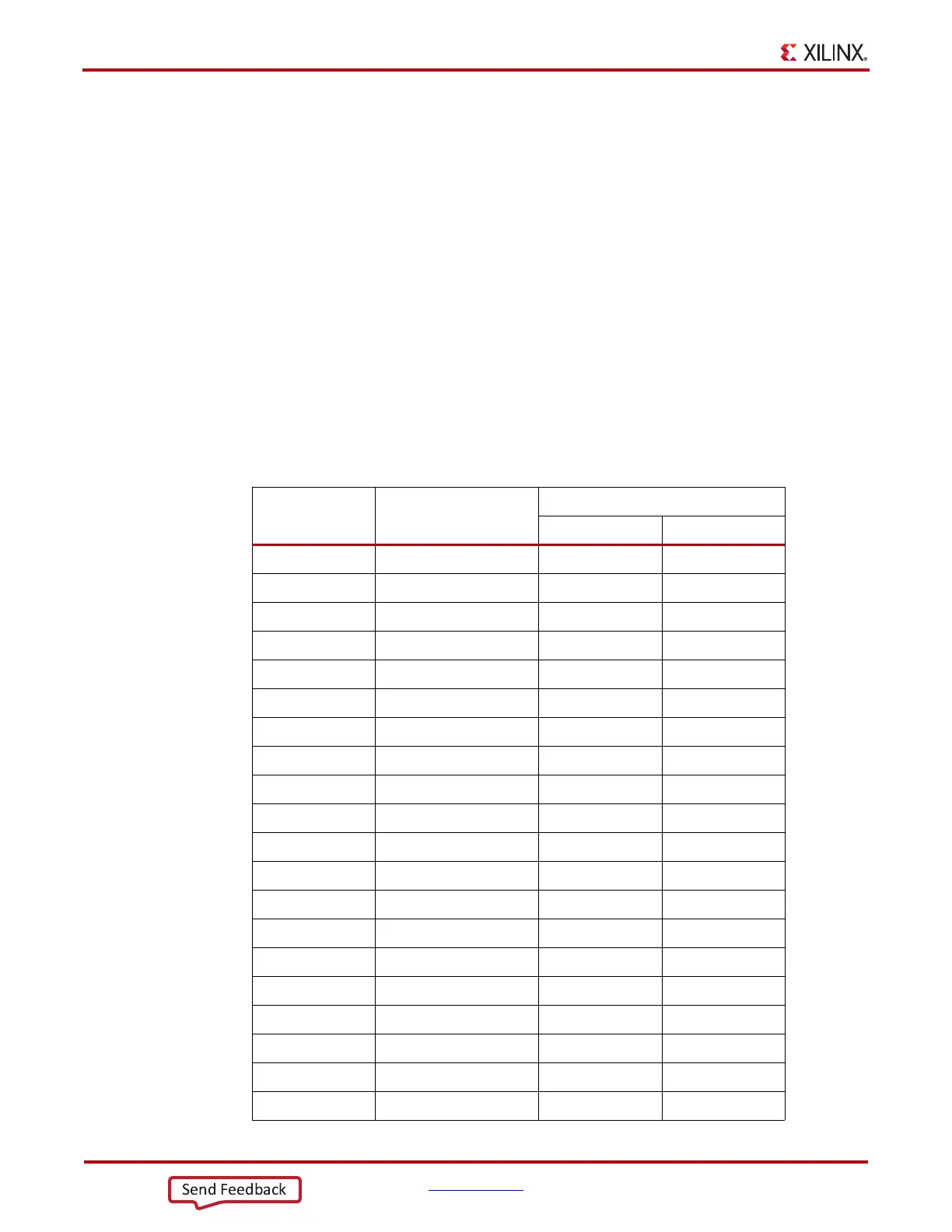
Table 1-4: DDR3 Memory Connections to the FPGA
FPGA (U1)
Pin
Net Name
J1 DDR3 Memory
Pin Number Pin Name
A20 DDR3_A0 98 A0
B19 DDR3_A1 97 A1
C20 DDR3_A2 96 A2
A19 DDR3_A3 95 A3
A17 DDR3_A4 92 A4
A16 DDR3_A5 91 A5
D20 DDR3_A6 90 A6
C18 DDR3_A7 86 A7
D17 DDR3_A8 89 A8
C19 DDR3_A9 85 A9
B21 DDR3_A10 107 A10/AP
B17 DDR3_A11 84 A11
A15 DDR3_A12 83 A12_BC_N
A21 DDR3_A13 119 A13
F17 DDR3_A14 80 A14
E17 DDR3_A15 78 A15
D21 DDR3_BA0 109 BA0
C21 DDR3_BA1 108 BA1
D18 DDR3_BA2 79 BA2
N14 DDR3_D0 5 DQ0