28 www.xilinx.com VC707 Evaluation Board
UG885 (v1.4) May 12, 2014
Chapter 1: VC707 Evaluation Board Features
Clock Generation
The VC707 board provides five clock sources for the FPGA. Table 1-9 lists the source
devices for each clock.
Table 1-10 lists the pin-to-pin connections from each clock source to the FPGA.
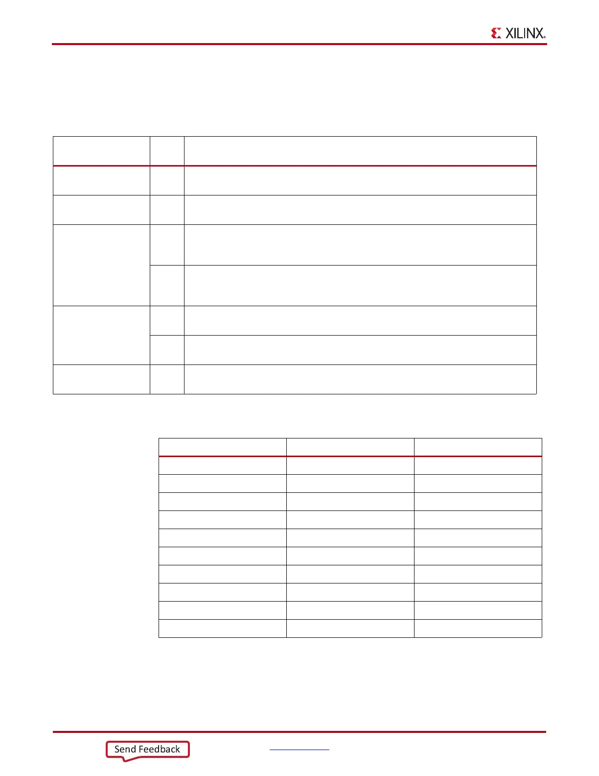
Table 1-9: VC707 Board Clock Sources
Clock Name
Clock
Source
Description
System Clock
U51
SiT9102 2.5V LVDS 200 MHz Fixed Frequency Oscillator (SiTime).
See System Clock (SYSCLK_P and SYSCLK_N), page 29
User Clock
U34
Si570 3.3V LVDS I
2
C Programmable Oscillator, 156.250 MHz default (Silicon Labs).
See Programmable User Clock (USER_CLOCK_P and USER_CLOCK_N), page 29
User SMA Clock
(differential pair)
J31
USER_SMA_CLOCK_P (Net name).
See User SMA Clock (USER_SMA_CLOCK_P and USER_SMA_CLOCK_N),
page 30.
J32
USER_SMA_CLOCK_N (Net name).
See User SMA Clock (USER_SMA_CLOCK_P and USER_SMA_CLOCK_N),
page 30.
GTX SMA REF Clock
(differential pair)
J25
SMA_MGT_REFCLK_C_P (Net name).
See GTX SMA Clock (SMA_MGT_REFCLK_P and SMA_MGT_REFCLK_N), page 31
J26
SMA_MGT_REFCLK_C_N (Net name).
See GTX SMA Clock (SMA_MGT_REFCLK_P and SMA_MGT_REFCLK_N), page 31
Jitter Attenuated
Clock
U24
Si5324C LVDS precision clock multiplier/jitter attenuator (Silicon Labs).
See Jitter Attenuated Clock, page 31
Table 1-10: Clock Connections, Source to FPGA
Clock Source Pin Net Name FPGA (U1) Pin
U51.5 SYSCLK_N E18
U51.4 SYSCLK_P E19
U34.5 USER_CLOCK_N AL34
U34.4 USER_CLOCK_P AK34
J26.1 SMA_MGT_REFCLK_N AK7
J25.1 SMA_MGT_REFCLK_P AK8
J32.1 USER_SMA_CLOCK_N AK32
J31.1 USER_SMA_CLOCK_P AJ32
U24.29 Si5324_OUT_N AD7
U24.28 Si5324_OUT_P AD8