VC707 Evaluation Board www.xilinx.com 31
UG885 (v1.4) May 12, 2014
Feature Descriptions
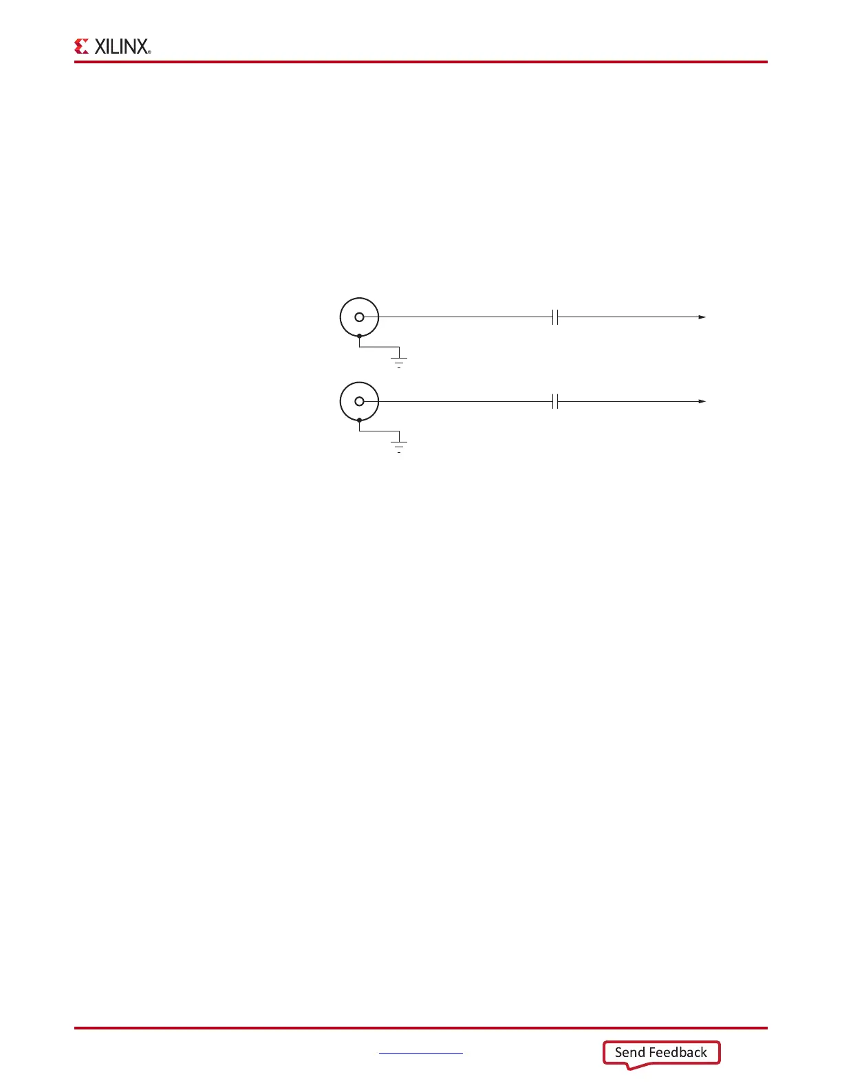
GTX SMA Clock (SMA_MGT_REFCLK_P and SMA_MGT_REFCLK_N)
[Figure 1-2, callout 10
The VC707 board includes a pair of SMA connectors for a GTX clock wired to GTX Quad
bank 113. This differential clock has signal names SMA_MGT_REFCLK_P and
SMA_REFCLK_N, which are connected to FPGA U1 pins AK8 and AK7 respectively.
Figure 1-12 shows this AC-coupled clock circuit.
• External user-provided GTX reference clock on SMA input connectors
• Differential Input
Jitter Attenuated Clock
[Figure 1-2, callout 11]
The VC707 board includes a Silicon Labs Si5324 jitter attenuator U24 on the back side of the
board. FPGA user logic can implement a clock recovery circuit and then output this clock
to a differential I/O pair on I/O bank 13 (REC_CLOCK_C_P, FPGA U1 pin AW32 and
REC_CLOCK_C_N, FPGA U1 pin AW33) for jitter attenuation. The jitter attenuated clock
(Si5324_OUT_C_P, Si5324_OUT_C_N) is then routed as a reference clock to GTX Quad 114
inputs MGTREFCLK0P (FPGA U1 pin AD8) and MGTREFCLK0N (FPGA U1 pin AD7).
The primary purpose of this clock is to support CPRI/OBSAI applications that perform
clock recovery from a user-supplied SFP/SFP+ module and use the jitter attenuated
recovered clock to drive the reference clock inputs of a GTX transceiver. The jitter
attenuated clock circuit is shown in Figure 1-13.
X-Ref Target - Figure 1-12
Figure 1-12: GTX SMA Clock Source
UG855_c1_12_020612
SMA_MGT_REFCLK_PSMA_MGT_REFCLK_C_P
SMA
Connector
J25
GND
C25
0.01 μF 25V
X7R
SMA_MGT_REFCLK_NSMA_MGT_REFCLK_C_N
SMA
Connector
J26
GND
C24
0.01 μF 25V
X7R