VC707 Evaluation Board www.xilinx.com 77
UG885 (v1.4) May 12, 2014
Configuration Options
Configuration Options
The FPGA on the VC707 board can be configured by the following methods:
• Master BPI (uses the Linear BPI Flash).
• JTAG (uses the USB-to-JTAG Bridge or Download cable). See USB JTAG, page 25 for
more information
See 7 Series FPGAs Configuration User Guide (UG470) [Ref 2] for further details on
configuration modes.
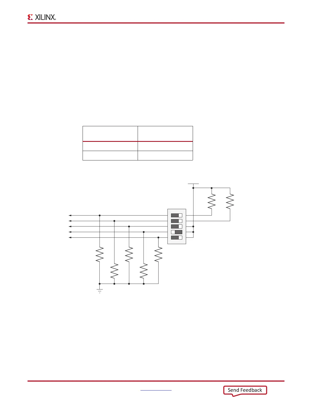
The method used to configure the FPGA is controlled by the mode pin (M2, M1, M0)
settings selected through DIP switch SW11. Table 1-34 lists the supported mode switch
settings.
Figure 1-36 shows mode switch SW13.
The mode pins settings on SW11 determine if the Linear BPI Flash is used for configuring
the FPGA. DIP switch SW11 also provides the upper two address bits for the Linear BPI
Flash and can be used to select one of multiple stored configuration bitstreams. Figure 1-37
shows the connectivity between the onboard nonvolatile Flash devices used for
configuration and the FPGA.
To obtain the fastest configuration speed an external 80 MHz oscillator is wired to the
EMCCLK pin of the FPGA. This allows users to create bitstreams that configure the FPGA
Table 1-34: Mode Switch SW11 Settings
Mode Pins
(M2, M1, M0)
Configuration Mode
010 Master BPI
101 JTAG
X-Ref Target - Figure 1-36
Figure 1-36: Mode Switch
UG885_c1_33_030512
SDA05H1SBD
SW11
R401
220Ω
0.1 W
1%
R402
220Ω
0.1 W
1%
VCC2V5
FPGA_M2
FPGA_M1
FPGA_M0
FLASH_A25
FLASH_A24
R396
1.21kΩ
0.1 W
1%
R397
1.21kΩ
0.1 W
1%
R398
1.21kΩ
0.1 W
1%
R399
1.21kΩ
0.1 W
1%
R400
1.21kΩ
0.1 W
1%
1
2
3
4
5
10
9
8
7
6
GND
ON