24 www.xilinx.com VC707 Evaluation Board
UG885 (v1.4) May 12, 2014
Chapter 1: VC707 Evaluation Board Features
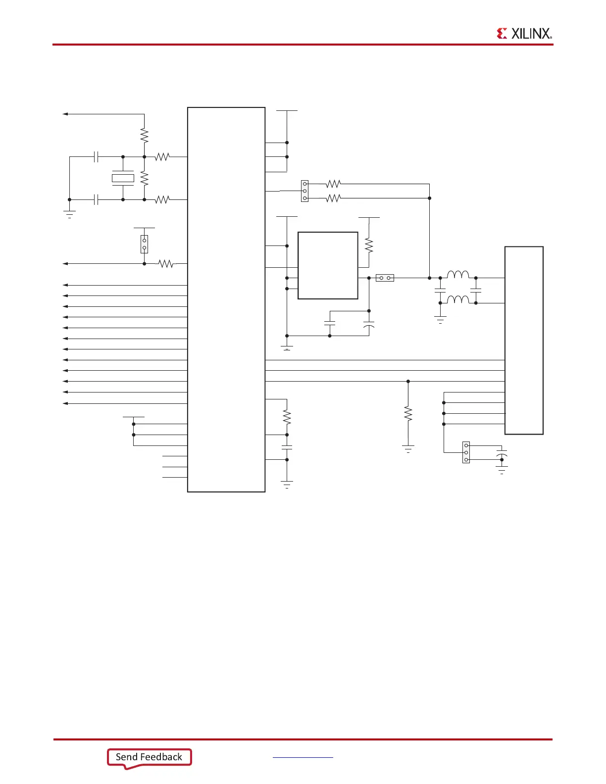
Figure 1-5 shows the USB 2.0 ULPI Transceiver circuitry.
SD Card Interface
[Figure 1-2, callout 5]
The VC707 board includes a secure digital input/output (SDIO) interface to provide
user-logic access to general purpose nonvolatile SDIO memory cards and peripherals. The
SD card slot is designed to support 50 MHz high speed SD cards.
The SDIO signals are connected to I/O bank 13 which has its VCCO set to 1.8V. A TI
TXB0108 8-bit bidirectional voltage-level translator (U31) is used between the FPGA and
the SD card connector (U29). Figure 1-6 shows the connections of the SD card interface on
the VC707 board.
X-Ref Target - Figure 1-5
Figure 1-5: USB 2.0 ULPI Transceiver
USB3320
USB 2.0
ULPI Transceiver
2
4
3
U8
1
5
DATA2
25
26
17
DATA1
DATA0
NXT
CLKOUT
REFCLK
XO
6
7
10
12
11
9
13
DATA7
NC
REFSEL1
DATA6
DATA5
DATA4
DATA3
19
18
23
21
24
20
VDD33_P
VBAT
RBIAS
ID
DP
DM
14
15
SPK_L
REFSEL2
33
CTR_GND
USB_SMSC_NXT
USB_SMSC_DATA0
USB_SMSC_DATA1
USB_SMSC_DATA2
USB_SMSC_DATA3
USB_SMSC_DATA4
UG885_c1_05_011813
R2
27.4 Ω
J14
VCC1V8
USB_SMSC_CLKOUT
VCC1V8
Connector,
USB Mini B
VBUS
D_N
GND
ID
D_P
J2
SHIELD
SHIELD
SHIELD
2
4
3
1
5
7
9
8
6
SHIELD
USB_SMSC_HEADER_N
USB_SMSC_HEADER_P
USB_SMSC_ID
3
1
2
GND
C326
Not
Installed
+
J44
16
SPK_R
8
REFSEL0
USB_SMSC_DATA5
USB_SMSC_DATA6
NC
USB_SMSC_DATA3
NC
NC
1
2X1
24.000 MHz
30 PPM
GND
C305
18 pF
C304
18 pF
TPS2051B
Power-Distribution
Switch
EN
IN
OC_B
U17
OUT
GND
5
4
1
2
3
R323
1 MΩ
R167
0Ω
R273
0Ω
L25 Ferrite 220
C104
0.1 μF
L26 Ferrite 220
C247
0.1 μF
GND
VCC5V0
CPEN
VCC3V3
R223
10 kΩ
R2
Not
Installed
GND
J13
C272
150 μF
C179
1 μF
+
GND
22
VBUS
1
3
2
J45
R222
10.0 kΩ
R291
1.00 kΩ
USB_SMSC_VBUS_SEL
USB_SMSC_REFCLK_OPTION
R249
DNP
VCC1V8
30
VDD18
GND
C282
2.2 μF
R323
1 MΩ
32
VDDIO
28
VDD18
31
27
29
RESETB
STP
DIR
USB_SMSC_DIR
USB_SMSC_STP
USB_SMSC_RESET
Default = No jumper
24 MHz
Default =
No jumper
Power from
USB host (J2)
Default =
jumper pins 1 - 2