VC707 Evaluation Board www.xilinx.com 23
UG885 (v1.4) May 12, 2014
Feature Descriptions
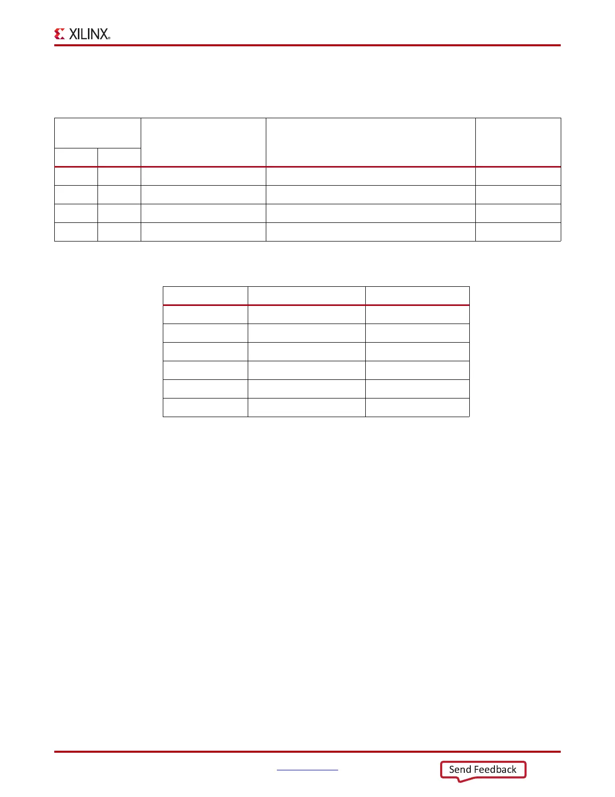
The connections between the USB mini-B connector at J2 and the PHY at U8 are listed in
Table 1-6.
The connections between the USB 2.0 PHY at U8 and the FPGA are listed in Table 1-7.
Table 1-6: USB Connector Pin Assignments and Signal Definitions Between J2 and U8
USB Connector
J2
Net Name Description
USB3320 (U8)
Pin
Pin Name
1 VBUS USB_SMSC_VBUS +5V from host system 22
2 D_N USB_SMSC_HEADER_N Bidirectional differential serial data (N-side) 19
3 D_P USB_SMSC_HEADER_P Bidirectional differential serial data (P-side) 18
4 GND USB_SMC_GND Signal ground 33
Table 1-7: USB 2.0 ULPI Transceiver Connections to the FPGA
FPGA (U1) Pin Net Name USB3320 (U8) Pin
AV36 USB_SMSC_DATA0 3
AW36 USB_SMSC_DATA1 4
BA34 USB_SMSC_DATA2 5
BB34 USB_SMSC_DATA3 6
BA36 USB_SMSC_DATA4 7
AT34 USB_SMSC_DATA5 9