60 www.xilinx.com VC707 Evaluation Board
UG885 (v1.4) May 12, 2014
Chapter 1: VC707 Evaluation Board Features
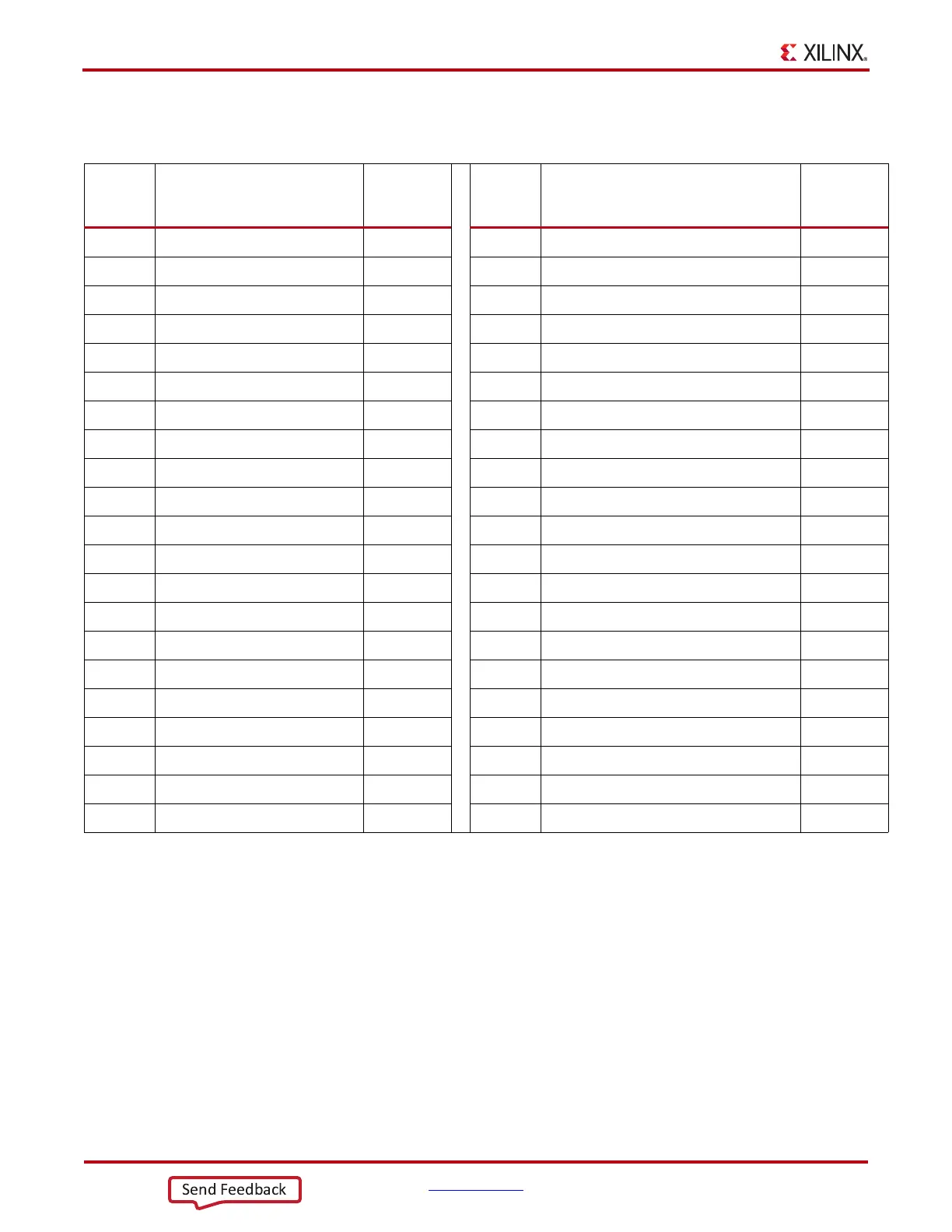
Table 1-27 lists the connections between the FMC1 HPC J35 connector and the FPGA U1.
Table 1-27: J35 VITA 57.1 FMC 1 HPC Connections
J35
FMC 1
HPC Pin
Schematic Net Name
U1 FPGA
Pin
J35
FMC 1
HPC Pin
Schematic Net Name
U1 FPGA
Pin
A2 FMC1_HPC_DP1_M2C_P C6 B1 NC
A3 FMC1_HPC_DP1_M2C_N C5 B4 NC
A6 FMC1_HPC_DP2_M2C_P B8 B5 NC
A7 FMC1_HPC_DP2_M2C_N B7 B8 NC
A10 FMC1_HPC_DP3_M2C_P A6 B9 NC
A11 FMC1_HPC_DP3_M2C_N A5 B12 FMC1_HPC_DP7_M2C_P E6
A14 FMC1_HPC_DP4_M2C_P H8 B13 FMC1_HPC_DP7_M2C_N E5
A15 FMC1_HPC_DP4_M2C_N H7 B16 FMC1_HPC_DP6_M2C_P F8
A18 FMC1_HPC_DP5_M2C_P G6 B17 FMC1_HPC_DP6_M2C_N F7
A19 FMC1_HPC_DP5_M2C_N G5 B20 FMC1_HPC_GBTCLK1_M2C_P E10
A22 FMC1_HPC_DP1_C2M_P D4 B21 FMC1_HPC_GBTCLK1_M2C_N E9
A23 FMC1_HPC_DP1_C2M_N D3 B24 NC
A26 FMC1_HPC_DP2_C2M_P C2 B25 NC
A27 FMC1_HPC_DP2_C2M_N C1 B28 NC
A30 FMC1_HPC_DP3_C2M_P B4 B29 NC
A31 FMC1_HPC_DP3_C2M_N B3 B32 FMC1_HPC_DP7_C2M_P F4
A34 FMC1_HPC_DP4_C2M_P J2 B33 FMC1_HPC_DP7_C2M_N F3
A35 FMC1_HPC_DP4_C2M_N J1 B36 FMC1_HPC_DP6_C2M_P G2
A38 FMC1_HPC_DP5_C2M_P H4 B37 FMC1_HPC_DP6_C2M_N G1
A39 FMC1_HPC_DP5_C2M_N H3 B40 NC