10 www.xilinx.com VC7203 GTX Transceiver Characterization Board
UG957 (v1.3) October 17, 2014
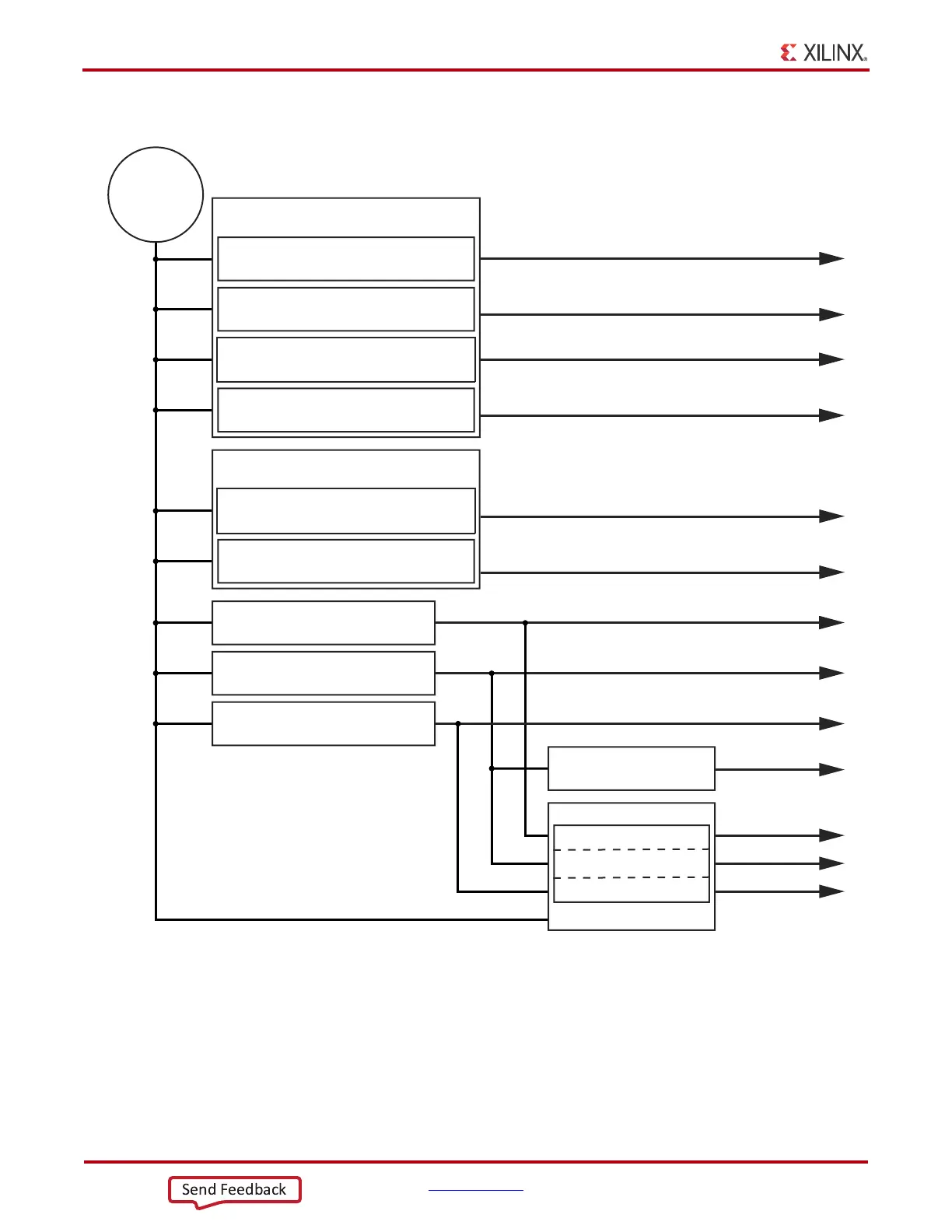
Chapter 1: VC7203 Board Features and Operation
X-Ref Target - Figure 1-3
Figure 1-3: VC7203 Board Power Supply Block Diagram
UG957_c1_03_100712
MGTVCCAUX
MGTAVTT
MGTAVCC
VCCAUX
VCCINT
VCCAUX_IO
VCCBRAM
VCCO_HR
VCCO_HP
Power Supply
12V PWR IN
J2 or J29
or J131
Power Controller 1
UCD9248PFC
U9
Switching Regulators (2 Phases)
1.0V at 40A max
U5, U51
Switching Regulator
1.8V at 10A max
U56Switching Regulator
1.0V at 10A max
Switching Regulator
1.8V at 10A max
U6
Power Controller 2
UCD9248PFC
U10
Switching Regulator
1.8V at 10A max
U57Switching Regulator
1.8V at 10A max
Switching Regulator
5.0V at 10A max
U2
Switching Regulator
3.3V at 18A max
U13
UTIL_5V0
UTIL_3V3
7 Series GTX Power Module
1.05V at 12.0A max
1.2V at 8.0A max
1.8V at 2.6A max
Linear Regulator
2.5V at 3A max
U62
VCCO_0
Switching Regulator
2.5V at 18A max
U52
UTIL_2V5
U50
U58
 Loading...
