VC7203 GTX Transceiver Characterization Board www.xilinx.com 17
UG957 (v1.3) October 17, 2014
Detailed Description
PROG_B Pushbutton
Pressing the PROG pushbutton SW3 (callout 14, Figure 1-2) grounds the active-Low
program pin of the FPGA.
DONE LED
The DONE LED DS21 (callout 12, Figure 1-2) indicates the state of the DONE pin of the
FPGA. When the DONE pin is High, DS21 lights indicating the FPGA is successfully
configured.
INIT LED
The dual-color INIT LED DS25 (callout 13, Figure 1-2) indicates the FPGA initialization
status. During FPGA initialization the INIT LED illuminates RED. When FPGA
initialization has completed the LED illuminates GREEN.
System ACE Tool SD Controller
The onboard System ACE tool SD controller U32 allows storage of multiple configuration
files on an SD card. These configuration files can be used to program the FPGA. The SD
card connects to the SD card connector J211 (callout 7, Figure 1-2) located directly below
the System ACE SD controller on the back side of the board.
System ACE Tool SD Controller Reset
Pressing the SASD RESET pushbutton SW7 (callout 9, Figure 1-2) resets the System ACE
tool SD controller. The reset pin is an active-Low input.
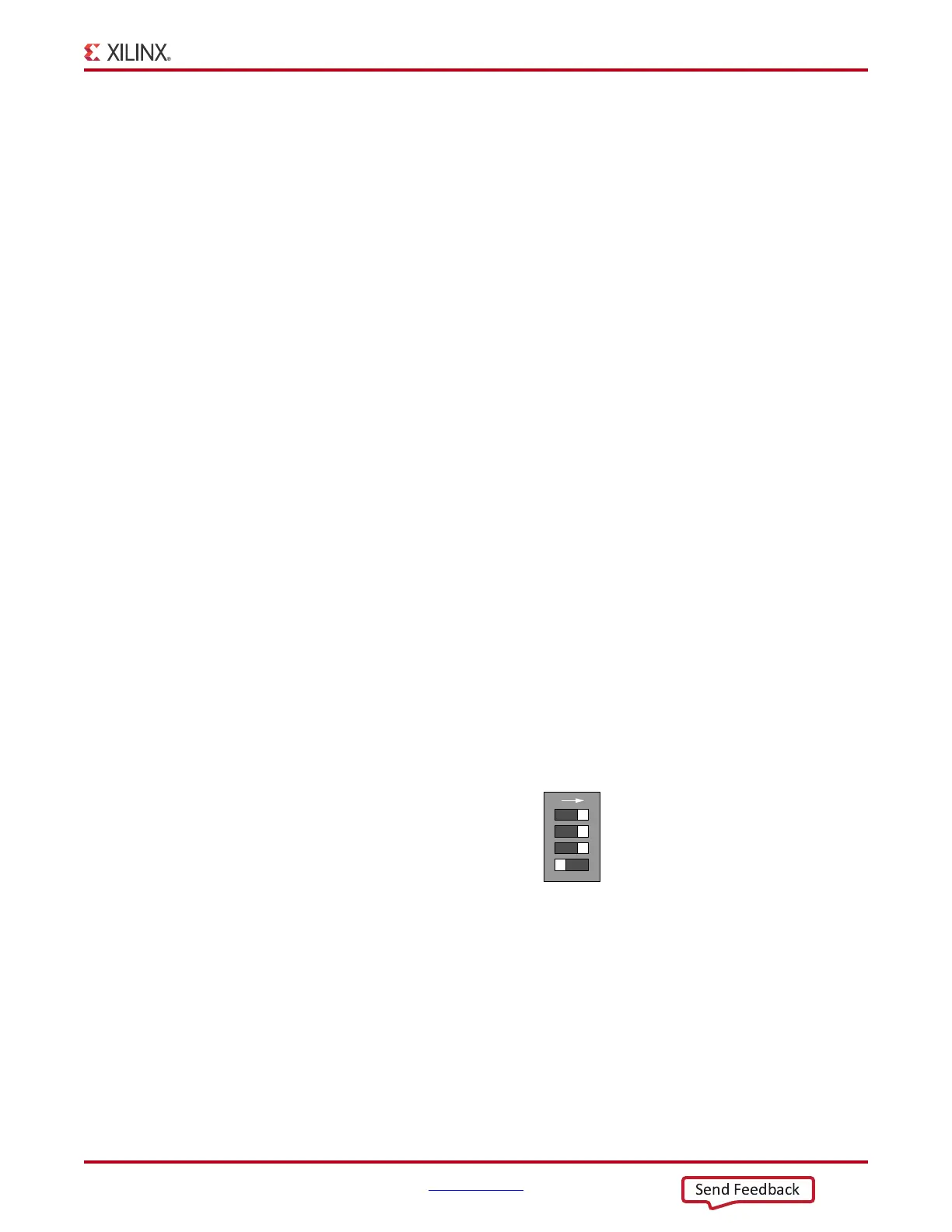
System ACE Tool SD Configuration Address DIP Switches
DIP switch SW8 shown in Figure 1-8 selects one of the eight configuration bitstream
addresses in the SD memory card. A switch is in the ON position if set to the far right and
in the OFF position if set to the far left. The MODE bit (switch position 4) is not used and
can be set either ON or OFF. SW8 is shown in Figure 1-2 as callout 8.
X-Ref Target - Figure 1-8
Figure 1-8: Configuration Address DIP Switch (SW8)
UG932_c1_08_100712
ADR0
ADR1
ADR2
2 3
4
SW8
1
MODE
ON
SYSACE-2 CFG
 Loading...

