VC7203 GTX Transceiver Characterization Board www.xilinx.com 19
UG957 (v1.3) October 17, 2014
Detailed Description
SuperClock-2 Module
Callout 10, Figure 1-2.
The SuperClock-2 module connects to the clock module interface connector (J82) and
provides a programmable, low-noise and low-jitter clock source for the VC7203 board. The
clock module maps to FPGA I/O by way of 24 control pins, 3 LVDS pairs, 1 regional clock
pair, and 1 reset pin. Table 1-9 shows the FPGA I/O mapping for the SuperClock-2 module
interface. The VC7203 board also supplies UTIL_5V0, UTIL_3V3, UTIL_2V5 and
VCCO_HR input power to the clock module interface.
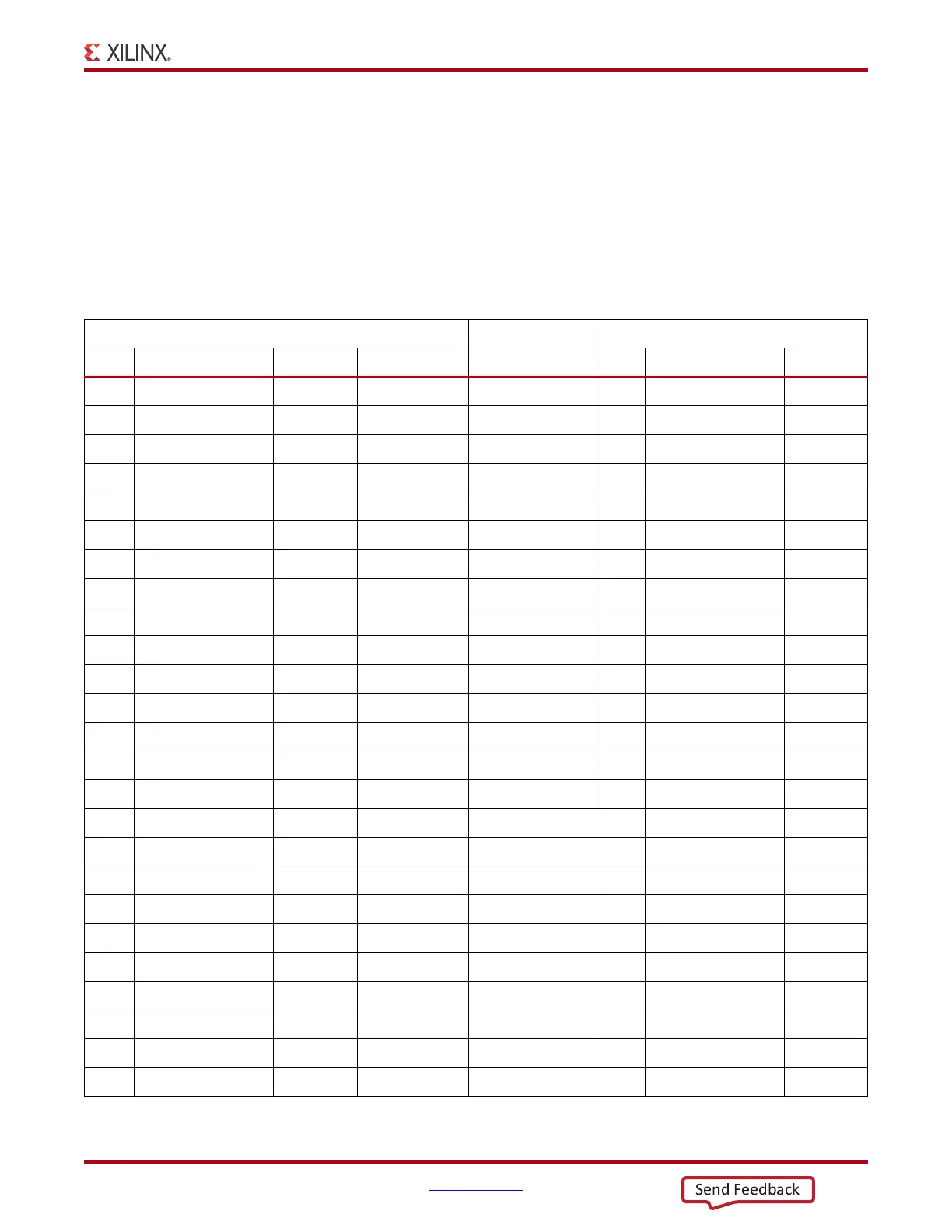
Table 1-9: SuperClock-2 FPGA I/O Mapping
FPGA (U1)
Schematic
Net Name
J82 Pin
Pin Function Direction I/O Standard Pin Function Direction
E12 Clock Recovery Input LVDS_25 CM_LVDS1_P 1 Clock Recovery Output
D12 Clock Recovery Input LVDS_25 CM_LVDS1_N 3 Clock Recovery Output
L12 Clock Recovery Input LVDS_25 CM_LVDS2_P 9 Clock Recovery Output
L11 Clock Recovery Input LVDS_25 CM_LVDS2_N 11 Clock Recovery Output
BA1 Clock Recovery Output LVDS CM_LVDS3_P 17 Clock Recovery Input
BB1 Clock Recovery Output LVDS CM_LVDS3_N 19 Clock Recovery Input
K19 Regional Clock Input LVDS_25 CM_GCLK_P 25 Global Clock Output
J18 Regional Clock Input LVDS_25 CM_GCLK_N 27 Global Clock Output
C19 Control I/O In/Out LVCMOS18 CM_CTRL_0 61 NC —
B19 Control I/O In/Out LVCMOS18 CM_CTRL_1 63 NC —
A16 Control I/O In/Out LVCMOS18 CM_CTRL_2 65 NC —
A15 Control I/O Output LVCMOS18 CM_CTRL_3 67 DEC Input
A20 Control I/O Output LVCMOS18 CM_CTRL_4 69 INC Input
A19 Control I/O Output LVCMOS18 CM_CTRL_5 71 ALIGN Input
B17 Control I/O In/Out LVCMOS18 CM_CTRL_6 73 NC —
A17 Control I/O In/Out LVCMOS18 CM_CTRL_7 75 NC —
B21 Control I/O In/Out LVCMOS18 CM_CTRL_8 77 NC —
A21 Control I/O In/Out LVCMOS18 CM_CTRL_9 79 LOL
C18 Control I/O Output LVCMOS18 CM_CTRL_10 81 INT_ALRM Input
B18 Control I/O Output LVCMOS18 CM_CTRL_11 83 C1B Input
D20 Control I/O Output LVCMOS18 CM_CTRL_12 85 C2B Input
C20 Control I/O Output LVCMOS18 CM_CTRL_13 87 C3B Input
F17 Control I/O Output LVCMOS18 CM_CTRL_14 89 C1A Input
E17 Control I/O Output LVCMOS18 CM_CTRL_15 91 C2A Input
D21 Control I/O In/Out LVCMOS18 CM_CTRL_16 93 NC —
 Loading...

