20 www.xilinx.com VC7203 GTX Transceiver Characterization Board
UG957 (v1.3) October 17, 2014
Chapter 1: VC7203 Board Features and Operation
User LEDs (Active-High)
Callout 23, Figure 1-2.
DS13 through DS20 are eight active-High LEDs that are connected to user I/O pins on the
FPGA as shown in Table 1-10 These LEDs can be used to indicate status or any other
purpose determined by the user.
User DIP Switches (Active-High) and I/O Header
Callout 25, Figure 1-2.
The DIP switch SW2 provides a set of eight active-High switches that are connected to user
I/O pins on the FPGA as shown in Table 1-11. These pins can be used to set control pins or
any other purpose determined by the user. Six of the eight I/Os also map to 2 x 6 test
header J125 providing external access for these pins (callout 26, Figure 1-2.).
C21 Control I/O Output LVCMOS18 CM_CTRL_17 95 CS0_C3A Input
D18 Control I/O Output LVCMOS18 CM_CTRL_18 97 CS1_C4A Input
D17 Control I/O In/Out LVCMOS18 CM_CTRL_19 99 NC —
F20 Control I/O In/Out LVCMOS18 CM_CTRL_20 101 NC —
E20 Control I/O In/Out LVCMOS18 CM_CTRL_21 103 NC —
K17 Control I/O In/Out LVCMOS18 CM_CTRL_22 105 NC —
J17 Control I/O In/Out LVCMOS18 CM_CTRL_23 107 NC —
J20 CM_RESET Output LVCMOS18 CM_RST 66 RESET_B Input
Table 1-9: SuperClock-2 FPGA I/O Mapping (Cont’d)
FPGA (U1)
Schematic
Net Name
J82 Pin
Pin Function Direction I/O Standard Pin Function Direction
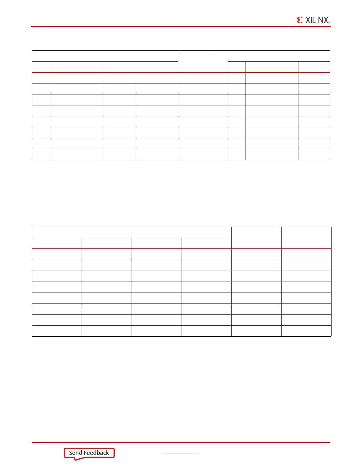
Table 1-10: User LEDs
FPGA (U1)
Schematic Net
Name
Reference
Designator
Pin Function Direction I/O Standard
M37 User LED Output LVCMOS18 APP_LED1 DS19
M38 User LED Output LVCMOS18 APP_LED2 DS20
R42 User LED Output LVCMOS18 APP_LED3 DS17
P42 User LED Output LVCMOS18 APP_LED4 DS18
N38 User LED Output LVCMOS18 APP_LED5 DS16
M39 User LED Output LVCMOS18 APP_LED6 DS15
R40 User LED Output LVCMOS18 APP_LED7 DS13
P40 User LED Output LVCMOS18 APP_LED8 DS14
 Loading...

