22 www.xilinx.com VC7203 GTX Transceiver Characterization Board
UG957 (v1.3) October 17, 2014
Chapter 1: VC7203 Board Features and Operation
GTX Transceivers and Reference Clocks
Callout 4, Figure 1-2.
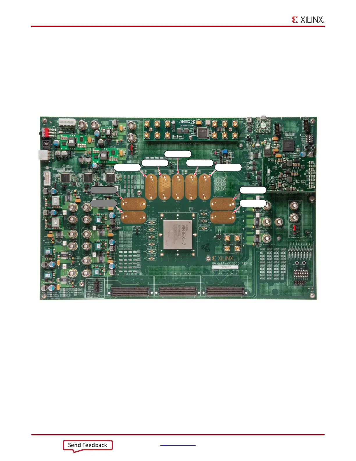
The VC7203 board provides access to all GTX transceiver and reference clock pins on the
FPGA as shown in Figure 1-10. The GTX transceivers are grouped into nine sets of four
RX-TX lanes. Four lanes are referred to as a Quad.
Note:
QUAD 111 and QUAD 112 do not connect to pins on the XCVX485T.
Note: Figure 1-10 is for reference only and might not reflect the current revision of the board.
Each GTX Quad and its associated reference clocks (CLK0 and CLK1) are brought out to a
connector pad which interfaces with Samtec BullsEye connectors used with the Samtec
HDR-155805-01-BEYE cable assembly. Contact Samtec, Inc. for information about this or
other cable assemblies. Figure 1-11 A shows the connector pad. Figure 1-11 B shows the
connector pinout.
X-Ref Target - Figure 1-10
Figure 1-10: GTX Quad Locations
UG957_c1_10_121613
QUAD_115
QUAD_116
QUAD_111
QUAD_112
QUAD_113
QUAD_118
QUAD_119
QUAD_117
QUAD_114
 Loading...

