VC7203 GTX Transceiver Characterization Board www.xilinx.com 7
UG957 (v1.3) October 17, 2014
Detailed Description
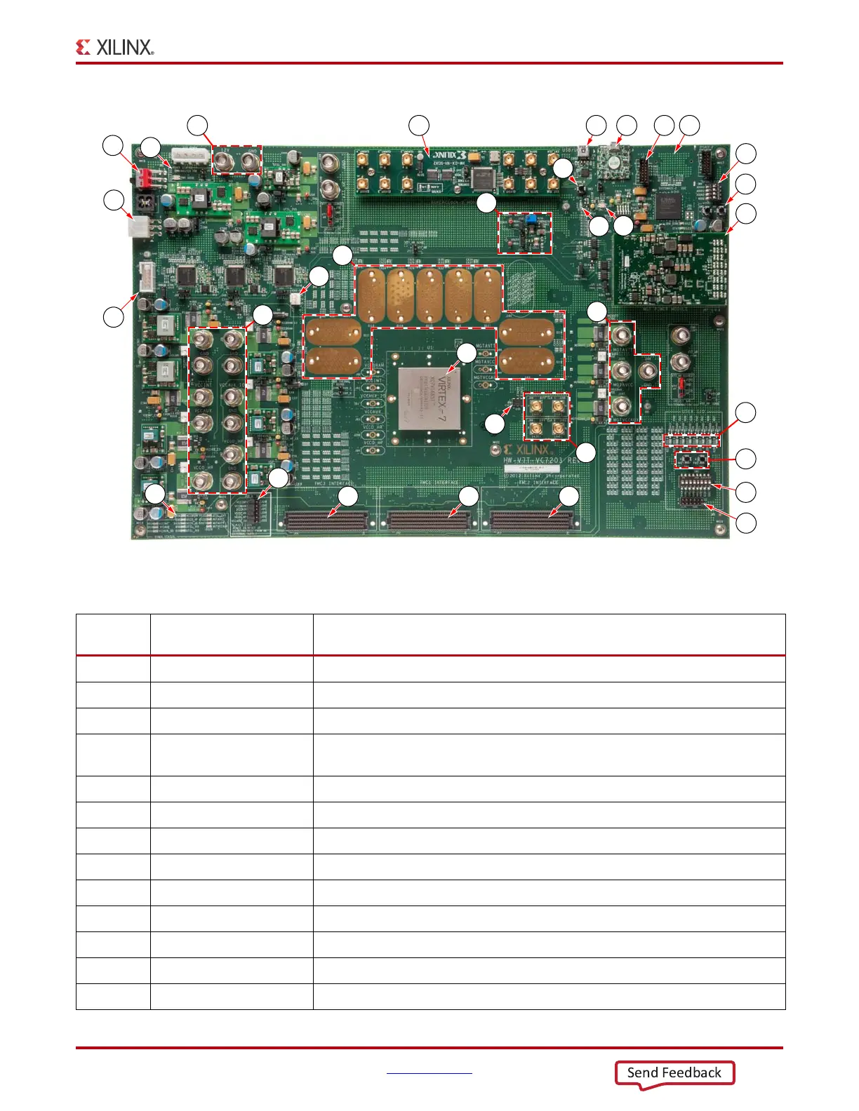
X-Ref Target - Figure 1-2
Figure 1-2: VC7203 Board Features. Callouts Listed in Table 1-1
Table 1-1: VC7203 Board Feature Descriptions
Figure 1-2
Callout
Reference Designator Feature Description
1 U1 Virtex-7 XC7VX485T-3 FFG1761E FPGA, page 15
2 SW1 Power switch, page 9
3 J2 12V Mini-Fit connector, page 8
4
J84, J85, J86, J158, J159,
J160, J161, J162, J163
GTX transceiver connector pads Q111 , Q112, Q113, Q114, Q115, Q116, Q117,
Q118 and Q119, page 22
5 U8 USB JTAG connector (micro-B receptacle), page 15
6 J7 JTAG connector (alternate access for programming cables), page 15
7 J211 System ACE tool SD card connector (back-side of board), page 15
8 SW8 System ACE tool SD configuration address DIP switches, page 17
9 SW7 System ACE tool SD RESET button, page 17
10 SuperClock-2 module, page 19
11 U35 200 MHz 2.5V LVDS oscillator, page 18
12 DS21 FPGA DONE status LED, page 17
13 DS25 FPGA INIT_B status LED, page 17
UG957_c1_02_100612
2
3
20
10
15
21
5
8
25
14
31
1
13
12
11
22
24
28
18
7
6
9
18
4
30
18
23
26
2729
17
16
19
 Loading...

