16 www.xilinx.com VC7203 GTX Transceiver Characterization Board
UG957 (v1.3) October 17, 2014
Chapter 1: VC7203 Board Features and Operation
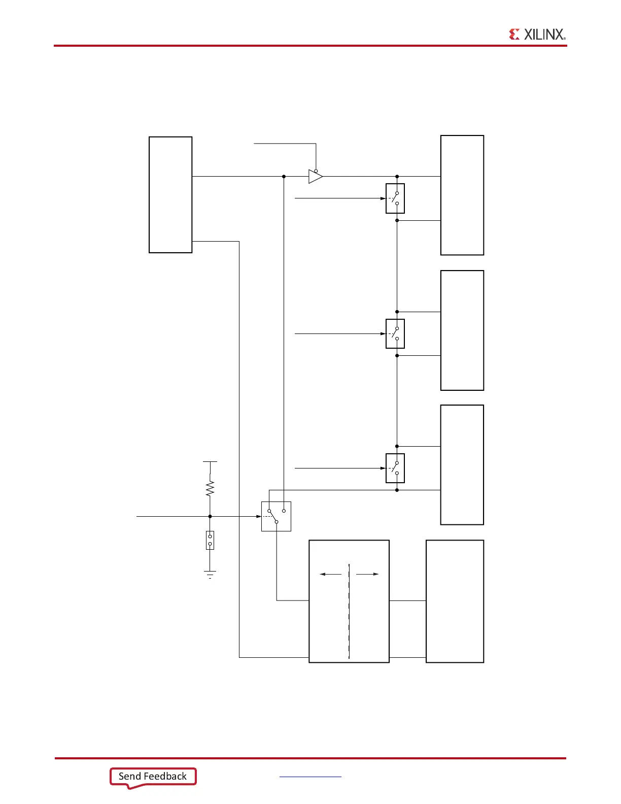
The JTAG chain of the board is illustrated in Figure 1-7. By default only the Virtex-7 FPGA
and the System ACE SD tool controller are part of the chain (J1 jumper OFF). Installing the
J1 jumper adds the FMC interfaces as well.
X-Ref Target - Figure 1-7
Figure 1-7: JTAG Chain
UG957_c1_07_100712
FMC1_PRSNT_M2C_L
FMC2_PRSNT_M2C_L
FMC1 HPC
Connector
TDI
TDO
JA2
FMC2 HPC
Connector
TDI
TDO
JA3
U7
Virtex-7
FPGA
TDI
TDO
U1
U8
Digilent
USB-JTAG
Module
TDI
TDO
System Ace SD
Controller
TDI
TDO
U32
CFGTDO
CFGTDI
U17
U12
FMC_JTAG_EN_B
U19
3.3V
2.5V
UTIL_3V3
10.0 K
J1
FMC3_PRSNT_M2C_L
FMC3 HPC
Connector
TDI
TDO
JA4
U17
FMC_JTAG_EN_B
 Loading...

