ZCU104 Board User Guide 23
UG1267 (v1.1) October 9, 2018 www.xilinx.com
Chapter 3: Board Component Descriptions
I/O Voltage Rails
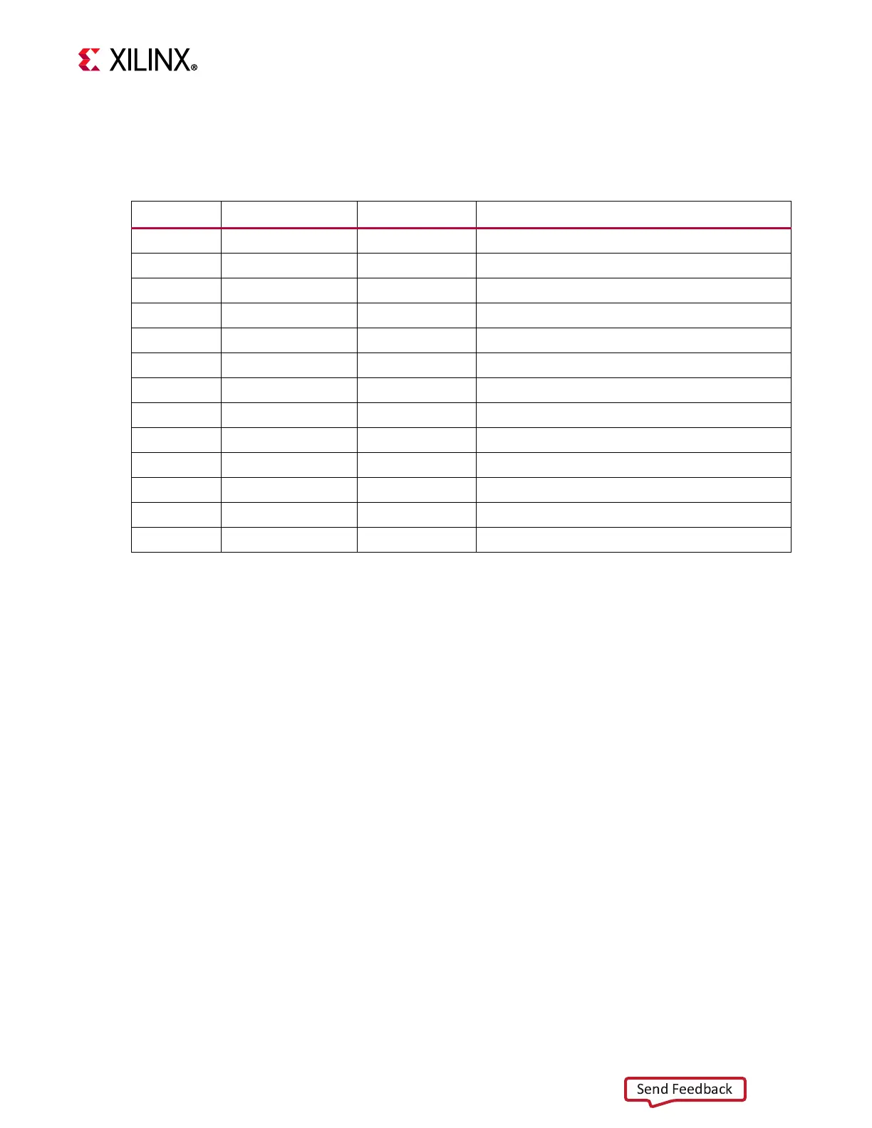
The XCZU7EV MPSoC PL I/O bank voltages on the ZCU104 board are listed in Figure 3-2.
Table 3-2: I/O Voltage Rails
XCZU7EV Power Net Name Voltage Connected To
PL Bank 28 V
CC1V8
1.8V UART2 only (mostly NC pins)
PL Bank 64 V
CC1V2
1.2V DDR4 SODIMM DQ[0:31] (PL)
PL Bank 65 V
CC1V2
1.2V DDR4 SODIMM DQ[32:63] (PL)
PL Bank 66 V
CC1V2
1.2V DDR4 SODIMM ADDR/CTRL (PL)
PL Bank 67 V
ADJ_FMC
(1)
1.8V FMC_LPC LA BUS
PL Bank 68 V
ADJ_FMC
(1)
1.8V FMC_LPC LA BUS
PL Bank 87 V
CC3V3
3.3V PMOD0, PMOD1, HDMI CTRL, PL_I2C1
PL Bank 88 V
CC3V3
3.3V HDMI, GPIO LED/DIP SW/PB SW
PS Bank 500 V
CC1V8
1.8V CAN, UART0/1, I2C0/1, QSPI LWR
PS Bank 501 V
CC1V8
1.8V SDIO, DP
PS Bank 502 V
CC1V8
1.8V ENET, USB_DATA[0:7], USB_CTRL
PS Bank 503 V
CC1V8
1.8V PS CONFIG I/F
PS Bank 504 V
CC1V2
1.2V DDR4 (4x16-BIT) 64-BIT COMPONENT I/F (PS)
Notes:
1. The ZCU104 board is shipped with V
ADJ_FMC
set to 1.8V.