ZCU104 Board User Guide 75
UG1267 (v1.1) October 9, 2018 www.xilinx.com
Chapter 3: Board Component Descriptions
Bank 505 DP (DisplayPort) lanes 0 and 1 TX support the 2-channel source only PS-side
DisplayPort circuitry described in DPAUX (MIO 27-30), page 55.
Bank 505 USB0 lane 2 supports the USB3.0 interface described in USB 3.0 Transceiver and
USB 2.0 ULPI PHY, page 35.
Bank 505 SATA1 lane 3 supports the M.2 SATA connector U170 as shown in Figure 3-7.
Bank 505 reference clocks are connected to the U182 8T49N287 clock generator as
described in Clock Generation, page 44.
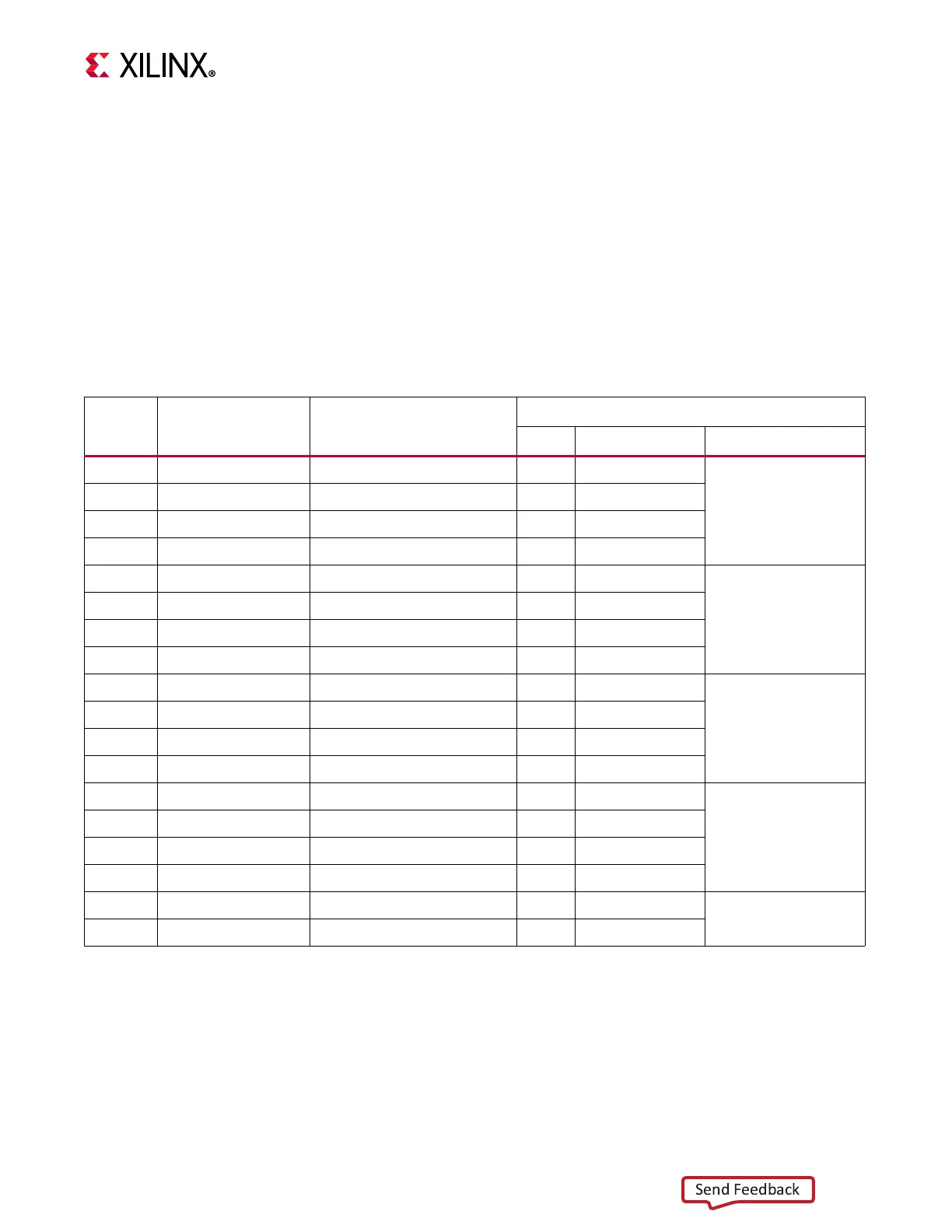
Bank 505 connections are shown in Table 3-28.
Table 3-28: PS-GTR Bank 505 Interface Connections
XCZU7EV
(U1) Pin
XCZU7EV Pin Name Schematic Net Name
(2)
Connected To
Pin No. Pin Name Device
U29 PS_MGTRTXP0 GT0_DP_TX_P
(1)
4 ML_LANE1_P
DisplayPort
connector P11
U30 PS_MGTRTXN0 GT0_DP_TX_N
(1)
6 ML_LANE1_N
R29 PS_MGTRTXP1 GT1_DP_TX_P
(1)
1 ML_LANE0_P
R30 PS_MGTRTXN1 GT1_DP_TX_N
(1)
3 ML_LANE0_N
U33 PS_MGTRRXP0 NC NA NA
NA
U34 PS_MGTRRXN0 NC NA NA
T31 PS_MGTRRXP1 NC NA NA
T32 PS_MGTRRXN1 NC NA NA
P31 PS_MGTRTXP2 GT2_USB0_TX_P
(1)
9SSTXP
USB J96
P32 PS_MGTRTXN2 GT2_USB0_TX_N
(1)
8 SSTXN
R33 PS_MGTRRXP2 GT2_USB0_RX_P 6 SSRXP
R34 PS_MGTRRXN2 GT2_USB0_RX_N 5 SSRXN
N29 PS_MGTRTXP3 GT3_SATA1_TX_P
(1)
2 SATA_A_P
M.2 U170
N30 PS_MGTRTXN3 GT3_SATA1_TX_N
(1)
3 SATA_A_N
N33 PS_MGTRRXP3 GT3_SATA1_RX_P
(1)
6 SATA_B_P
N34 PS_MGTRRXN3 GT3_SATA1_RX_N
(1)
5 SATA_B_N
T27 PS_MGTREFCLK0P NC NA NA
NA
T28 PS_MGTREFCLK0N NC NA NA