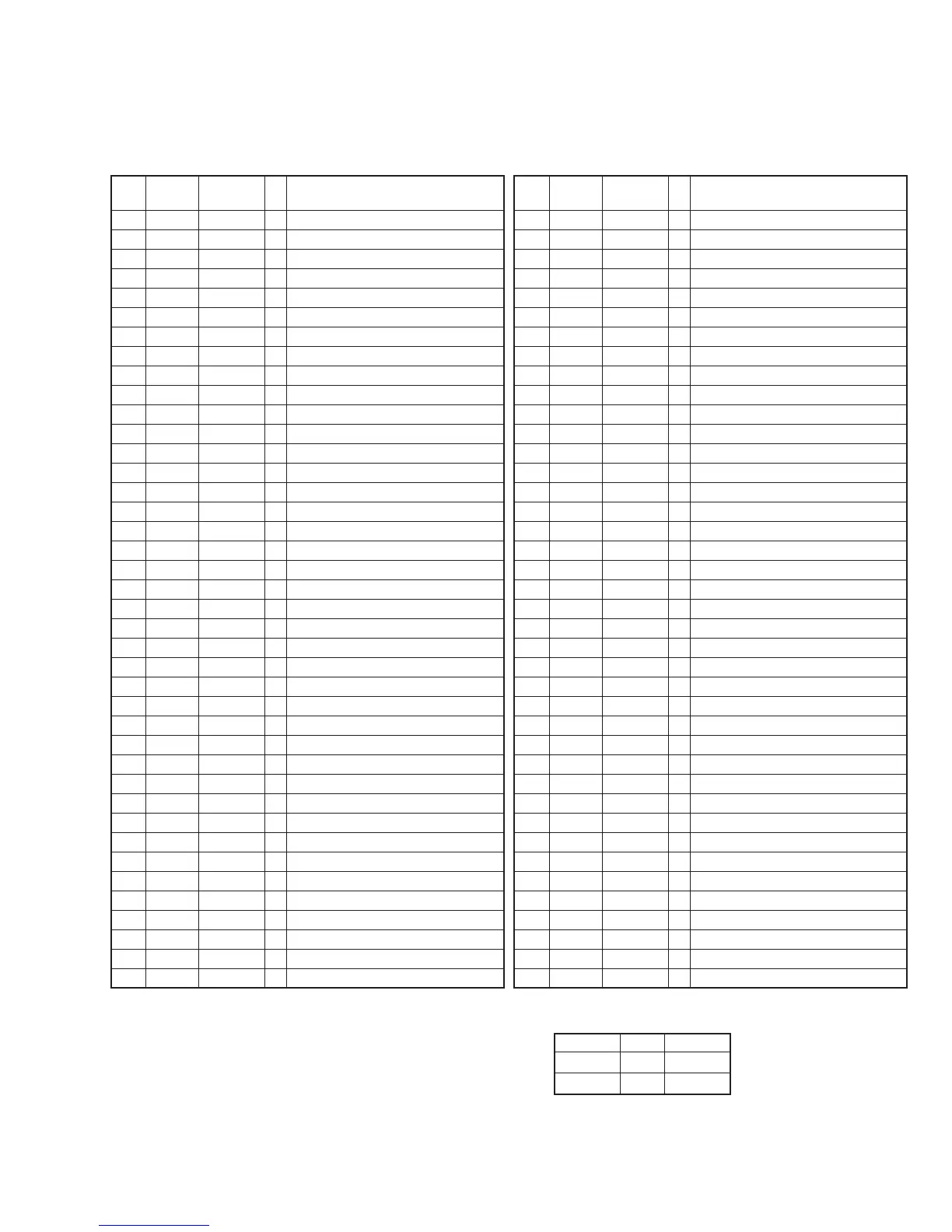
24
DSP-A595a
Pin Pin
Port I/O Function
No. Name
1 PA3 CDO I Receive data from DIR2
2 PA4 /ICDI O Initial clear for DIR2
3 PA5 /KM1 O Switching DIR2 forced (analog) mode
4 P70/INT0 LOCKN IRQ PLL lock flag
5 P71/INT1 ERRD IRQ DIR 2 error detect
6 P72/INT2 ERRA IRQ AC3D2av mute detect
7 P73/INT3 NONPCM IRQ AC3D2av AC-3 data detect
8 /RES /RES – Reset from Main µ-COM
9 XT1 XT1 I Connected to VDD1
10 XT2 XT2 I Unconnected
11 VSS1 VSS1 G Ground
12 CF1 CF1 Ø
Ceramic Oscillator Connected (10kHz)
13 CF2 CF2 Ø
Ceramic Oscillator Connected (10kHz)
14 VDD1 VDD1 +5V +5V power supply
15 P80/AN0 NC O Unconnected
16 P81/AN1 NC O Unconnected
17 P82/AN2 NC O Unconnected
18 P83/AN3 NC O Unconnected
19 P84/AN4 NC O Unconnected
20 P85/AN5 NC O Unconnected
21 P86/AN6 NC O Unconnected
22 P87/AN7 NC O Unconnected
23 P30 /ICAK O Initial clear for CODEC AD/DA
24 P31 CEAK O Chip enable for CODEC AD/DA
25 P32 /ICAC O Initial clear for AC3D2av
26 P33 CEAC2 O Chip enable 2 for AC3D2av
27 P34 CEAC1 O Chip enable 1 for AC3D2av
28 P10/SO0 TXAC TX
Transmit data for AC3D2av and CODEC AD/DA
29 P11/SI0 RXAC RX Receive data from AC3D2av
30
P12/SCK0
CLKAC CLK
Clock for AC3D2av and CODEC AD/DA
31 P13/SO1 RSRV Ipu Not used (Normal)
32 P14/SI1 TRXOB I/O Not used (Normal)
33
P15/SCK1
CLKOB I Not used (Normal)
34
P16/PWM
NC I Unconnected
35
P17/PWM
NC I/O Unconnected
36 SO2 STM TX Transmit data for Main µ-COM
37 SI2 MTS RX Receive data from Main µ-COM
38 SCK2 CKIF
RXCK
Clock from Main µ-COM
39 SI2P3 WCIF O Clock for Main µ-COM
40 PWM1 TRQ O Transmit request for Main µ-COM
Pin Pin
Port I/O Function
No. Name
41 PWM0 NC OL Unconnected
42 VDD2 VDD2
+5V
+5V power supply
43 VSS2 VSS2 G Ground
44 P00 NC I/O Unconnected
45 P01 NC I/O Unconnected
46 P02 NC I/O Unconnected
47 P03 NC I/O Unconnected
48 P04 NC I/O Unconnected
49 P05 NC I/O Unconnected
50 P06 NC I/O Unconnected
51 P07 NC I/O Unconnected
52
P20/INT4
NC I/O Unconnected
53
P21/INT4
NC I/O Unconnected
54
P22/INT4
NC I/O Unconnected
55
P23/INT4
NC I/O Unconnected
56
P24/INT5
NC I/O Unconnected
57
P25/INT5
NC I/O Unconnected
58
P26/INT5
NC I/O Unconnected
59
P27/INT5
NC I/O Unconnected
60 PB7 NC I/O Unconnected
61 PB6 NC I/O Unconnected
62 PB5 NC I/O Unconnected
63 PB4 DSP Ipu Connected to VSS3
64 PB3 MUTO Ipu Unconnected (Fixed H)
65 PB2 LDC/O I LD Coaxial/Optical detect
66 PB1 CDC/O I Fixed H
67 PB0 RF Ipu Connected to VSS3 (Switched L)
68 VSS3 VSS3 G Ground
69 VDD3 VDD3
+5V
+5V power supply
70 PC7 NC I/O Unconnected
71 PC6 NC I/O Unconnected
72 PC5 VER Ipu Connected to VSS3 (Switched L)
73 PC4 DRB O Unconnected
74 PC3 DRA O Unconnected
75 PC2 DIC O Unconnected
76
PC1 DIB O Digital input selector control B
∗1
77
PC0 DIA O Digital input selector control A
∗1
78
PA0 DMT O L/R D/A converter mute
79
PA1 CLD O Chip select for DIR2
80
PA2 CCK O Serial clock for DIR2
IC14 : LC875164A-5K20
8 bit Sub
µ-COM
∗1 Digital input selector control
Hi = 1, Low = 0
Input DIB DIA
DVD/LD 0 0
TV/DBS 1 0
 Loading...