P1 1a a 1a a a a a a a a a a a a
16G 15G 14G 13G 12G 11G 10G 9G 8G 4G 3G 2G 1G
P2 1b b 1b b b b b b b b b b b b
P3 1c c 1c c c c c c c c c c c c
P4 1d d 1d d d d d d d d d d d d
P5 1e e 1e e e e e e e e e e e e
P6 1f f 1f f f f f f f f f f f f
P7 1g g 1g g g g g g g g g g g g
P8 1h h 1h h h h h h h h h h h h
P9 1j j 1j j j j j j j j j j j j
P101kk1kkk kkkkkkkkk
P111mm1mmm mmmmmmmmm
P121nn1nnn nnnnnnnnn
P131pp1ppp ppppppppp
P14 1r r 1r r r r r r r r r r r r
P15 – – t t t t t t t t
P16 2a 2a – – – – – – – –
P17 2b,2c
(PTY)
2b B1 – –
P18 2d 2c B2 – –
P19 2e,2f
(RT)
2d B3 – S1 – – –
P20 2g 2e B4 S2 – – – – –
P21 2j,2p
(CT)
2f B5
(PS)
– –––––
P22 2m 2g S3 – – – – – – –
7G
~5G
(Left)
(Right)
31
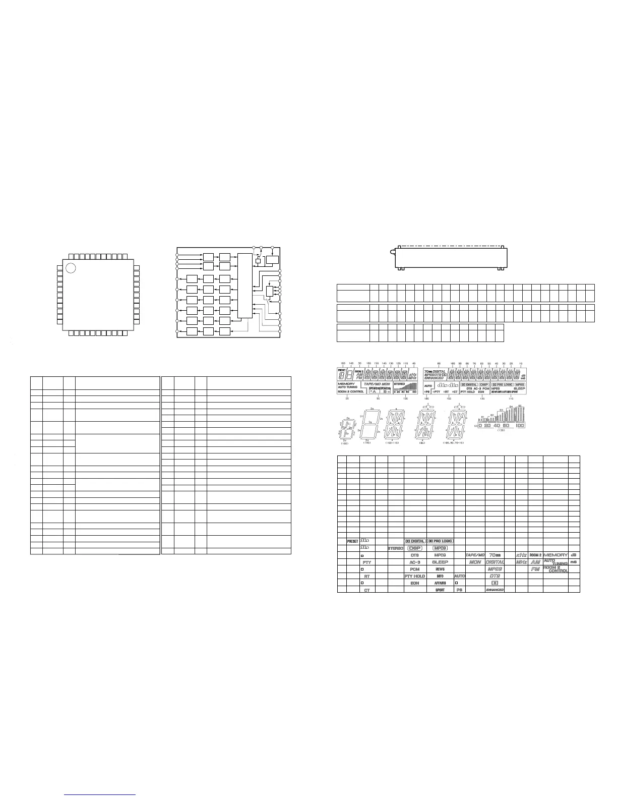
IC6 : AK4526A-VQ (CODEC AD/DA)
20 bit 6 channel A/D, D/A Converter
VR
VR
VR
VR
VR
VR
LPF DAC
LPF DAC
LPF DAC
LPF DAC
LPF DAC
LPF DAC
SDOS
OCKS
M/S
BICK
LRCK
SDTI1
SDTI2
SDTI3
SDTO
DAUX
DFS
DEM1
DEM0
MCKO
DVDD
DVSS
/PD
XTS
ICKS1
ICKS0
CAD1
CAD0
CDTO
CDTI
CCLK
/CS
P/S
MCKI
XTI
AVSS
AVDD
VREFH
VCOM
VREFL
RIN+
RIN–
LIN+
LIN–
ROUT1
LOUT1
ROUT2
LOUT2
ROUT3
LOUT3
1
2
3
4
5
6
7
8
9
10
11
12
13
14
15
16
17
18
19
20
21
22
34
35
36
37
38
39
40
41
42
43
44
23
24
25
26
27
28
29
30
31
32
33
13
12
11
1
6
9
7
8
25
26
23
24
DEM0
10
DAUX
SDIN3
SDIN2
SDIN1
SDOUT
BICK
LRCK
MCLK
DEM1
2
14
OCKS
MCKO
DFS
SDTO
SDOS
SDTI1
LOUT2
LOUT2
28
ROUT1
27
LOUT1
31
RIN–
ROUT2
ROUT3
SDTI2
SDTI3
TOP VIEW
39
5
4
MCKI
LRCK
BICK
32
RIN+
29
LIN–
30
LIN+
1/2
Audio
I/F
ADC HPF
DEM
Clock Gen.
ADC HPF
Pin Pin
I/O Function
No. Name
1 SDOS I Connected to ground (digital)
2 OCKS I Connected to ground (digital)
3 M/S I Connected to ground (digital)
4 BICK I/O
Audio serial data clock,
bit clock input from Main µ-COM
5 LRCK I/O
Input/Output channel clock,
word clock input from Main µ-COM
6 SDTI1 I
DAC Audio serial data input 1-3,
PCM input from AC3D2av
7 SDTI2 I
8 SDTI3 I
9 SDTO O
Audio serial data output,audio
data for DIR2
10 DAUX I Connected to ground (digital)
11 DFS I Connected to ground (digital)
12 DEM1 I
Connected to ground (digital)
13 DEM0 I
14 MCKO O Unconnected
15 DVDD Power supply (digital)
16 DVSS Ground (digital)
17 /RD I Power down and reset, initial clear
from Sub µ-COM
18 XTS I Connected to ground (analog)
19 ICKS1 I Connected to ground (analog)
20 ICKS0 I Connected to ground (analog)
21 CAD1 I Connected to ground (analog)
22 CAD0 I Connected to ground (analog) 44 CDTO O Unconnected
Pin Pin
I/O Function
No. Name
23 LOUT3 O
O
Lch analog output 3, for CENTER
Rch analog output 3, for LFE
24 ROUT3
25 LOUT2 O
O
Lch analog output 2, for REAR
26 ROUT2 Rch analog output 2, for REAR
27 LOUT1 O Lch analog output 1, for FRONT
28 ROUT1 O Rch analog output 1, for FRONT
29 LIN– I Lch analog negative input, from MAIN
30 LIN+ I Lch analog positive input, from MAIN
31 RIN– I Rch analog negative input, from MAIN
32 RIN+ I Rch analog positive input, from MAIN
33 VREFL I Connected to ground (analog)
34 VCOM O Common voltage output
35 VREFH I
I
Connected to power supply (analog)
36 AVDD Power supply (analog)
37 AVSS Ground (analog)
38 XTI Unconnected
39 MCKI
External master clock input, FsX256
Bit clock from DIR2
40 P/S I Connected to ground (digital)
41 /CS I
Chip select in serial mode, chip enable
from Sub µ-COM
42 CCLK I
Control data clock in serial mode,
clock from Sub µ-COM
43 CDTI I
Control data input in serial mode,
Tramsmit data from Sub µ-COM
 Loading...