EasyManuals Logo

Zynq UltraScale+ User Manual

Zynq UltraScale+
70 pages
To Next Page IconTo Next Page
To Previous Page IconTo Previous Page
Page #41 background imageLoading...
Page #41 background image
RFSoC Data Converter Evaluation Tool User Guide 41
UG1287 (v2018.2) October 1, 2018 www.xilinx.com
Chapter 5: Evaluation Tool System Configuration using the GUI
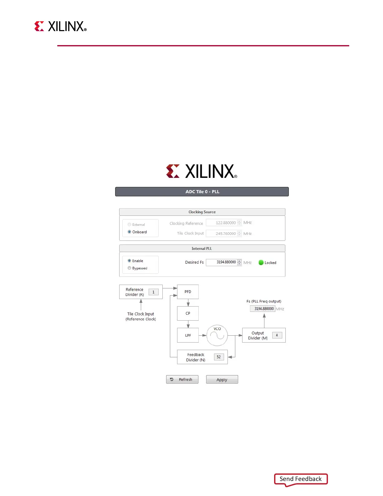
ADC Clock Configuration
The GUI supports:
Selection of external or internal (PLL) sample clock options
On-chip PLL configuration for internal sample clock generation (see Figure 5-5).
The configuration of the RF PLLs on the evaluation board for external clocking
Note:
RFPLL (LMK) is also used to set up the reference clock for the on-chip PLLs. The nominal
settings are 245.76 MHz or 491.52 MHz, for example.
X-Ref Target - Figure 5-5
Figure 5-5: ADC Internal PLL
X21282-092118
Send Feedback

Questions and Answers:

Question and Answer IconNeed help?

Do you have a question about the Zynq UltraScale+ and is the answer not in the manual?

Zynq UltraScale+ Specifications

General IconGeneral
Max TransceiversUp to 32
Transceiver SpeedUp to 32.75 Gbps
FamilyZynq UltraScale+
Processor CoresQuad-core ARM Cortex-A53, Dual-core ARM Cortex-R5
Max MemoryDDR4
Power ConsumptionVaries by configuration, typically 10W to 30W
Operating TemperatureIndustrial (-40°C to +100°C), Extended (-40°C to +125°C)
Package OptionsVarious BGA packages
CategoryFPGA SoC