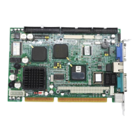
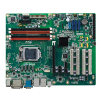
PCA-6781 User Manual 28
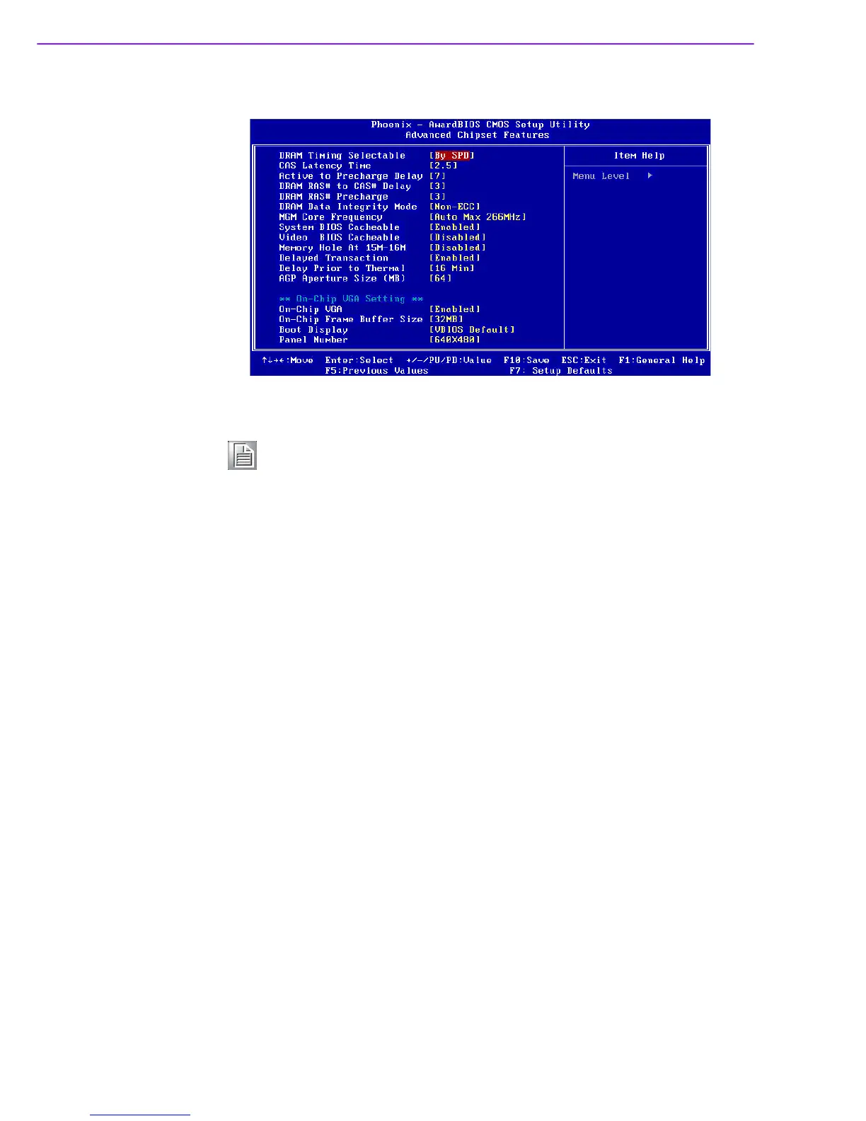
3.2.4 Advanced Chipset Features
! DRAM Timing Selectable [By SPD]
This item enables users to set the optimal timings for items 2 through 5, system
default setting of “By SPD” to follow the SPD information and ensure the system
running in stable and optimal performance.
! CAS Latency Time[2.5]
This item enables users to set the timing delay in clock cycles before SDRAM
start a read command after receiving it.
! Active to Precharge Delay[7]
This item enables users to control the memory back’s minimum row active time
(tRAS), system default is setting to “7” to reference value.
! DRAM RAS# to CAS# Delay[3]
This item enables users to set the timing of the transition from RAS (row
address strobe) to CAS (column address strobe) as both rows and column are
separately addressed shortly after DRAM is refreshed.
! DRAM RAS# Precharge[3]
This item enables users to set the DRAM RAS# precharge timing, system
default is setting to “3” to reference value.
! DRAM Data Integrity Mode [Non-ECC]
This item enables users to set the DRAM Type of Error data correction, system
default is setting to “Non-ECC” to reference value.
! MGM Core Frequency [Auto Max 266 MHz]
This item enables users to set the operation speed of internal Graphic Chip FSB
and DRAM, system default is setting to “Auto Max 266 MHz” to reference value.
! System BIOS Cacheable [Enabled]
This item allows the system BIOS to be cached to allow faster execution and
better performance.
Note! This "Advanced Chipset Features" option controls the configuration of
the board's chipset, and can be used to fine tune performance. This
page is chipset dependent; screen may vary according to chipset
installed. It is strongly recommended that only technical users make
changes to the default settings.