NOTE
IF A POWER SUPPLY PROBLEM SEEMS INTERMITTENT, GENTLY TAPPING THE HVPS WITH A
SCREWDRIVER WILL INDUCE THE PROBLEM FOR TEST PURPOSES.
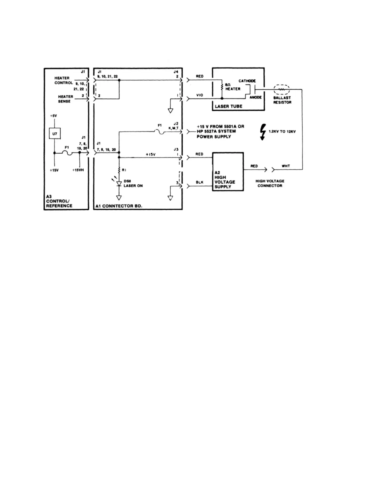
Figure 8-17. High
Voltage Power
Supply, Schematic Diagram
8-90. A3 CONTROLLER/REFERENCE BD & A4 SAMPLER BD CIRCUIT THEORY 8-91.
Introduction
8-92.
Figure 8-22
shows the schematic diagram for the A3 Controller/Reference Board and the A4 Sampler
Board.
8-93. The Al, A3, and A4 boards contain the electronics for the following portions of the Laser Head Block Diagram:
• Power Amplifier
• Warmup Error Amplifier
• Photodiode and Amplifier
• Liquid Crystal
• Clock and State Machine
• Subtracting Sample and Hold
• Reference Receiver
8-94. Clock (A)
8-95. The frequency of oscillator A3U10 is determined by timing components A3R8, C3, C7, and C8. For normal
operation, A3C7 gives an output frequency of approximately 100 Hz. For testing purposes, capacitors A3C3, C7, and
C8 can be configured so that the oscillator circuit generates a 1000 Hz output (JMP 8 in HI position). To
troubleshoot using signature analysis, the oscillator can be configured to run at 75 kHz (±20%) by removing the
CLOCK FREQUENCY jumper (JMP 8) completely.
8-96. Dividers (B)