1-107
Troubleshooting
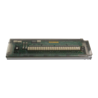
RF Path Description (Frequency Generation, Level Control, and Modulation)
Level accuracy is a function of the detector and instrument calibration. Because the instrument is
calibrated with internal detectors, external level accuracy depends on the voltage difference
between the internal and external detectors at any given RF power level and the difference in
linearity between the internal and external detectors.
When internally leveled, the ALC circuit is temperature compensated to improve level accuracy
over the specified temperature range. Temperature compensation for the A25 Highband Detector
consists of a temperature sensing circuit on the A24 Highband Coupler. A resistor pack calibrates
the A25 Highband Detector; if the A25 Highband Detector is replaced, a new resistor pack is
provided with the new detector, and must be installed on the A24 Highband Coupler. Although rare,
unstable level performance above 2 GHz can be the result of problems with poorly soldered resistors
on the resistor pack, or with other components in the temperature compensation circuit.
The A23 Lowband Coupler Detector temperature correction circuit is inside the A23 Lowband
Coupler Detector package. Because the lowband detector and coupler are in one package, they
cannot be replaced independently.
Modulation (AM, FM, ΦM, and Pulse)
Modulation features apply only to certain models and options of signal generators. The A11
Pulse/Analog Modulation Generator provides modulation signals for AM, FM, pulse, and phase, and
SYNC OUT and VIDEO OUT signals. For phase synchronization and modulation accuracy, a dual
function generator on the A11 Pulse/Analog Modulation Generator is tied to the 10 MHz reference
from A7 Reference. Pulse Input, EXT1, and EXT2 provide external modulation input connections. A
front panel low frequency output connector (LF Output) can be selected to output the signal
generated by the A11 Pulse/Analog Modulation Generator to drive other instruments.
EXT 1 and EXT 2 inputs contain modulation drive level detection circuits that generate error
messages if the signal applied to the input is too small or too large. The input impedance of EXT 1
and EXT 2 can be set for 50 or 600 ohms, and can be configured for dc or ac coupling.
AM
The AM signal from the A11 Pulse/Analog Modulation Generator is routed to the A10 ALC, where it
is summed with the ALC reference voltage to drive the A30 Modulation Filter and A8 Output ALC
diodes.
FM/
ΦM
The FM/
ΦM modulation signal is routed from the A11 Modulation Generator to the A6 Frac–N. On
the A6 Frac–N:
• FM rates <4 kHz are applied to the pre-scale control circuit and the A6 Frac–N VCO. This
generates a change in the pre-scaled drive (feedback from the VCO) to the VCO’s phase detector,
causing a VCO frequency change.
• FM rates 4 to 100 kHz are applied only to the A6 Frac–N VCO.
• FM rates >100 kHz are routed from the A6 Frac–N to the A9 YIG Driver and applied to the FM
coil in the YIG Oscillator.
• For phase modulation, the FM drive signal is routed through an LCR circuit Other than the LCR
circuit,
ΦM signals are routed the same as FM signals.