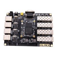
ARTIX-7 FPGA Development Board AX7101 User Manual
Part 1: FPGA Development Board Introduction
The entire structure of the AX7101 FPGA development board is inherited
from our consistent “core board + carrier board” model. A high-speed
inter-board connector is used between the core board and the carrier board.
The core board is mainly composed of FPGA + 2 DDR3 + QSPI FLASH,
which undertakes the functions of high-speed data processing and storage of
FPGA, high-speed data reading and writing between FPGA and two DDR3s,
data bit width is 32 bits, and the bandwidth of the whole system is up to 25Gb.
/s(800M*32bit); The two DDR3 capacities are up to 8Gbit, which meets the
need for high buffers during data processing. The selected FPGA is the
XC7A100T chip of XILINX's ARTIX-7 series, in BGA 484 package. The
communication frequency between the XC7A100T and DDR3 reaches 400Mhz
and the data rate is 800Mhz, which fully meets the needs of high-speed
multi-channel data processing. In addition, the XC7A100T FPGA features four
GTP high-speed transceivers with speeds up to 6.6Gb/s per channel, making it
ideal for fiber-optic communications and PCIe data communications.