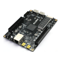
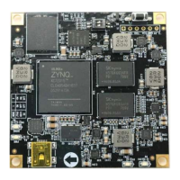
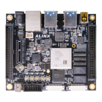
ARTIX-7 FPGA Development Board AX7101 User Manual
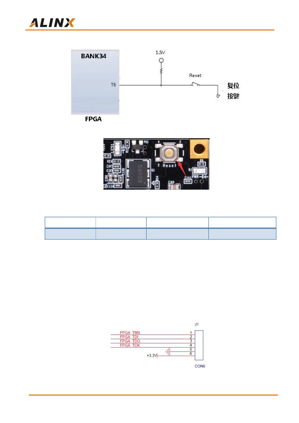
the reset key connection is shown in Figure 2-7-1:
Figure 2-7-1: Reset key Schematic
Figure 2-7-2: Reset key on the Core Board
Reset key pin assignment
Part 2.8: JTAG Interface
The JTAG test socket J1 is reserved on the AC7100B core board for JTAG
download and debugging when the core board is used alone. Figure 2-8-1 is
the schematic part of the JTAG port, which involves TMS, TDI, TDO, TCK. ,
GND, +3.3V these six signals.
Figure 2-8-1: JTAG Interface Schematic


 To Next Page