Component Test Procedures 2-9
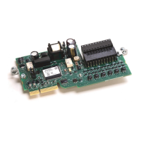
Gate Interface Resistance
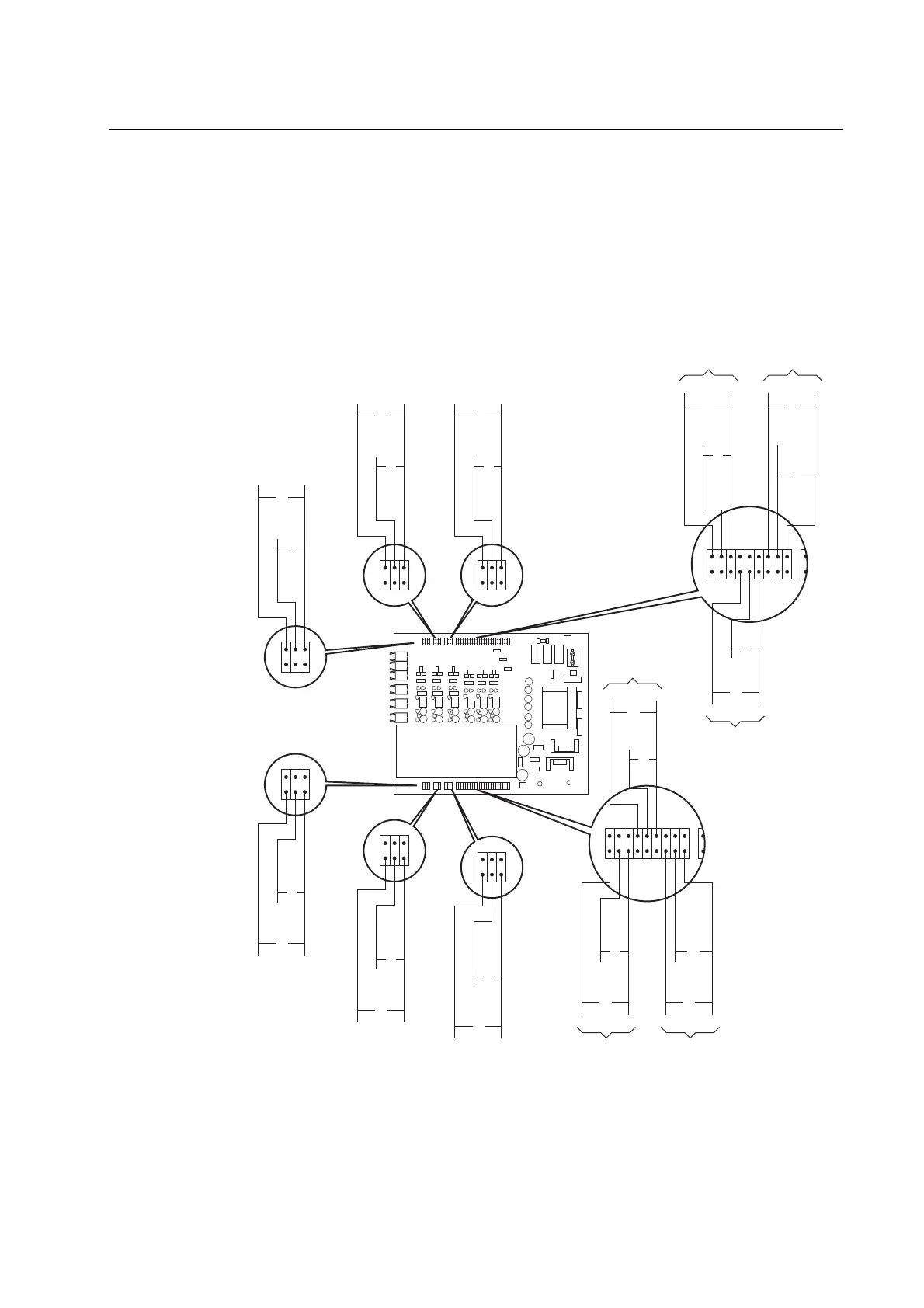
Measure the gate interface resistance for each output power transistor. The
resistance from each gate and collector pin to the branch emitter pin should
be about 500 ohms. If any of the gate interfaces fails this test, replace the
appropriate (left or right) Output Power Module per Power Structure.
H5H7H9H4H6H8
X3
X4
X5
X6
X7
X8
X9
X10
X11
X12
X13
X14
X15
X1
X3
~500 ohms
~500 ohms
Emitter
Gate Interface for W High (WH)
in Left Power Output Module
X4
~500 ohms
~500 ohms
Emitter
Gate Interface for V High (VH)
in Left Power Output Module
X5
~500 ohms
~500 ohms
Emitter
Gate Interface for U High (UH)
in Left Power Output Module
X6
~500 ohms
~500 ohms
~500 ohms
~500 ohms
~500 ohms
~500 ohms
Gate Interface
for W Low (WL)
in Left Power
Output Module
Gate Interface
for U Low (UL)
in Left Power
Output Module
Gate Interface
for V Low (VL)
in Left Power
Output Module
X8
~500 ohms
~500 ohms
Emitter
Gate Interface for W High (WH)
in Right Power Output Module
X9
~500 ohms
~500 ohms
Emitter
Gate Interface for V High (VH)
in Right Power Output Module
X10
~500 ohms
~500 ohms
Emitter
Gate Interface for U High (UH)
in Right Power Output Module
X11
~500 ohms
~500 ohms
~500 ohms
~500 ohms
~500 ohms
~500 ohms
Gate Interface
for W Low (WL)
in Left Power
Output Module
Gate Interface
for U Low (UL)
in Left Power
Output Module
Gate Interface
for V Low (VL)
in Left Power
Output Module
 Loading...