P54x/EN ST/La4 Settings
(ST) 4-26
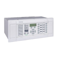
MiCOM P543, P544, P545, P546
ST
Setting range
Menu text Default setting
Min. Max.
Step size
Aid. 1 DeltaTrip 3 Pole 1 or 3 Pole
Setting that defines tripping mode for Aided 1 Delta.
This setting is visible only if tripping mode under GROUP x LINE PARAMETERS/ Trip
d 3 pMode is set to 1 an ole.
tREV. Guard 0.02 s 0 s 0.15 s 0.002 s
S line,
w
T
etting for the current reversal guard timer. Intended to keep stability on a healthy
hilst breakers open on a faulted parallel line to clear the fault.
his setting is visible only when over-reaching or Blocking schemes are selected.
Send on Trip Aided/Z1 Aided/Z1, Any None Trip or
Setting that defines the reinforced trip signal for POR Aided 1 scheme.
If selected to: None: No reinforced signal is issued
Aided/Z1: The reinforced signal is issued with aided trip or with Z1 if
aided distance scheme is enabled
Any Trip: Signal is reinforced with Any trip (DDB 522)
Weak Infeed Disabled Disabled, Echo, or Echo and Trip
Setting that defines Aided 1 scheme operation in case of weak infeed conditions, where no
ote relay, “Trip” will allow local end tripping after a set delay.
protection elements detect the fault at the local end, but an aided channel has been
received from the remote end. Setting “Echo” will allow the received signal to be returned
to the rem
WI Sngl Pole Trp Disabled Disabled or Enabled
Setting that defines the Weak Infeed tripping mode. When disabled, any WI trip will be
converted to a 3 phase trip.
WI V< Thresh. 45 V 10 V 70 V 5 V
Setting of Weak Infeed level detector. If phase - ground voltage in any phase drops below
t d with in phase current for the protection to operate, the end is
d eak infee l.
he threshold an
eclared as a w
sufficient
d termina
WI Trip Delay 0.06 s 0 s 1 s 0.002 s
Setting for the weak infeed trip time delay.
Custom Send Mask 0000000001
Bit 0 = Z1 Gnd, Bit 1 = Z2 Gnd, Bit 2 = Z4
Gnd, Bit 3 = Z1 Ph, Bit 4 = Z2 Ph,
Bit 5 = Z4 Ph, Bit 6 = DEF Fwd,
Bit 7 = DEF Rev, Bit
L sending a
p line end. For the signal to be sent, the element must operate
a onding bit in the matrix must be se (High).
the operation e.
This setting is visible only if a Programmable or
ogic Settings that determine the element or group of elements that are
ermissive signal to the other
nd a corresp t to 1
The above mapping is part of a custom made Aided 1 scheme, and unlike all other
schemes that are factory tested, the customer must take the responsibility for testing and
of the schem
Prog. Unblocking scheme is selected.
Custom Time PU 0 s 0 s 1 s 0.002 s
P of DD Custom e the
time delay elapses, the DDB signal ‘Aid1 Custo
ick up time delay B signal ‘Aid1 T in’, available in the PSL logic. Onc
mT out’ will become high.
Custom Time DO 0 s 0 s 1 s 0.002 s
Drop off time delay of DDB signal ‘Aid1 CustomT in’. Once the time delay elapses, the
DDB signal ‘Aid1 CustomT out’ will become low.
Note: The timer is a combined hard coded PU/DO timer for Custom Aided scheme 1.
 Loading...