Firmware Design P54x/EN FD/La4
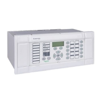
MiCOM P543, P544, P545 & P546
(FD) 9-7
2.4 Input module
The in
put module provides the interface between the relay processor board and the analog
and digital signals coming into the relay. The input module consists of two or three PCBs;
the main input board and one or two transformer board(s). The P543 and P545 relays use
one transformer board to provide four voltage inputs and five current inputs. The P544 and
P546 relays use two transformer boards to provide five voltage inputs and eight current
inputs.
2.4.1 Transformer board
The
current inputs will accept either 1 A or 5 A nominal current (observe menu and wiring
options) and the nominal voltage input is 100/110/115/120 V.
The transformers are used both to step-down the currents and voltages to levels appropriate
to the relay’s electronic circuitry and to provide effective isolation between the relay and the
power system. The connection arrangements of both the current and voltage transformer
secondaries provide differential input signals to the main input board to reduce noise.
2.4.2 Input board
The main inp
ut board is shown as a block diagram in Figure 2. It provides the circuitry for
the digital inp
ut signals and the analog-to-digital conversion for the analog signals. Hence it
takes the differential analog signals from the CTs and VTs on the transformer board(s),
converts these to digital samples and transmits the samples to the processor board via the
serial data bus. On the input board the analog signals are passed through an anti-alias filter
before being multiplexed into a single analog to digital converter chip. The A - D converter
provides 16-bit resolution and a serial data stream output. The digital input signals are opto
isolated on this board to prevent excessive voltages on these inputs causing damage to the
relay's internal circuitry.
VT
CT
VT
CT
Diffn
to
single
Diffn
to
single
Low
pass
filter
Low
pass
filter
Buffer
16-bit
ADC
Optical
isolator
Noise
filter
Buffer
Serial
Interface
Sample
control
16:1
Multiplexer
Anti-alias filters
Transformer board
Input board
Up to 8 current inputs
4 voltage inputs
8 digital inputs
Parallel bus
Serial sample
data bus
Trigger from processor
board
Parallel bus
Diffn
to
single
Low
pass
filter
Diffn
to
single
Low
pass
filter
Optical
isolator
Noise
filter
Up to 8 Up to 8
Up to 8
4 4 4
8
8
P0127ENf
Calibration
E PROM
2
FD
Figure 2 Main input board
Three spare channels are used to sample three different reference voltages for the purpose
of continually checking the operation of the multiplexer and the accuracy of the A-D
converter. The sample rate is maintained at 48 samples per cycle of the power waveform by
a logic control circuit which is driven by the frequency tracking function on the main
processor board.
 Loading...