A–2 Appendix A: Programming Flash Memory
CFI Flash Memory
Cyclone V SoC Development Kit May 2013 Altera Corporation
User Guide
Programming CFI Flash Using the Quartus II Programmer
You can use the JTAG interface in Altera CPLDs to indirectly program the flash
memory device. The Altera CPLD JTAG block interfaces directly with the logic array
in a special JTAG mode. This mode brings the JTAG chain through the logic array
instead of the Altera CPLD boundary-scan cells (BSC). The PFL megafunction
provides JTAG interface logic to do the following:
■ Convert the JTAG stream provided by the Quartus II software.
■ Program the CFI flash memory devices connected to the CPLD I/O pins.
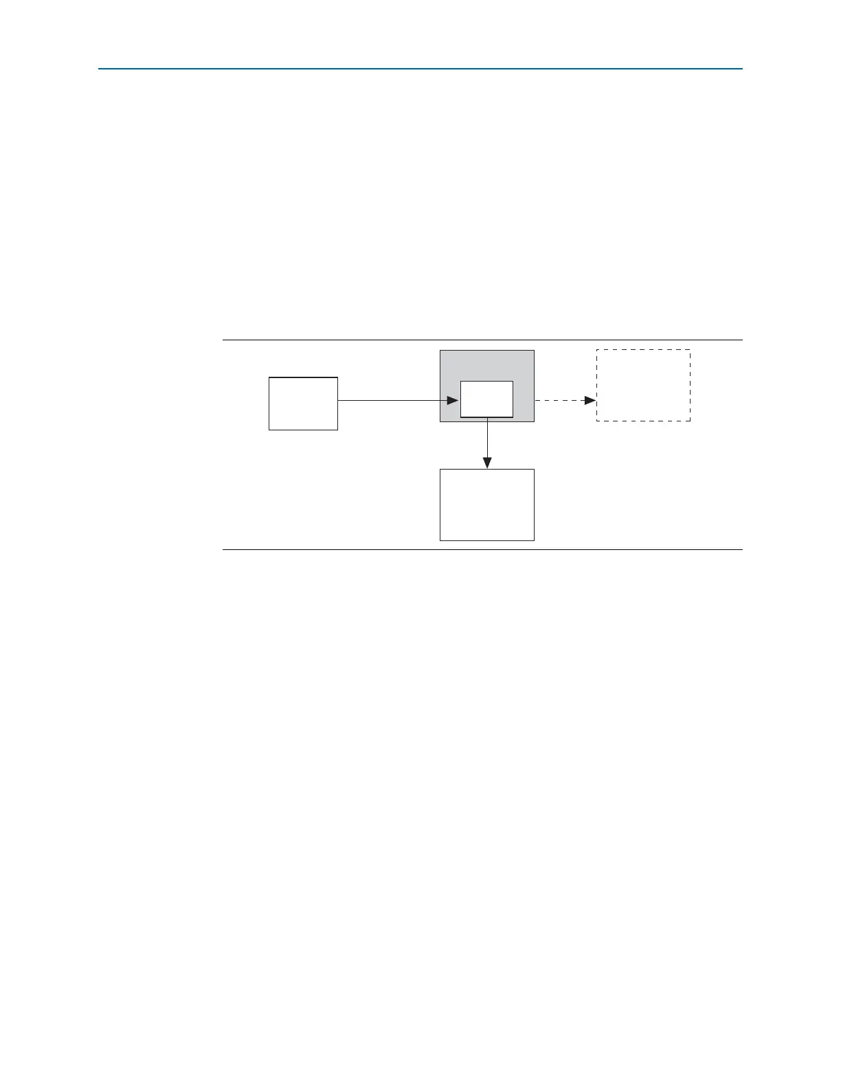
Figure A–1 shows an Altera CPLD configured as a bridge to program the CFI flash
memory device through the JTAG interface.
Perform the following steps to program a user design to the flash device in the
Quartus II Programmer:
1 The following flash writing procedure blinks the SEL 2, 1, and 0 LEDs and does not
support the Power Monitor, Clock Control, or other logic functions. It should only be
used for configuration.
1. On the To ols menu in the Quartus II software, click Programmer.
2. In the Programmer window, click Auto-Detect.
1 If you do not see USB Blaster or the board's embedded USB Blaster II listed
next to Hardware Setup, refer to the “Installing the USB-Blaster II Driver”
on page 3–3.
3. Click Add File and open <install
dir>\kits\cycloneVSX_5csxfc6df31es_soc\factory_recovery\max2_PFL_writer.
pof.
4. Turn on the Program/Configure option for the .pof file.
5. Click Start to download the selected configuration file to the MAX V CPLD.
Configuration is complete when the progress bar reaches 100%
6. Click Auto Detect and a flash device should show up attached to the MAX V in
the main window.
Figure A–1. Programming the CFI Flash Memory With the JTAG Interface
MAX II CPLD
CFI Flash
Memory
Altera
FPGA
Configuration Data
Common
Flash
Interface
PFL
Quartus II
Software
via JTAG
Altera FPGA Not Used
for Flash Programming