UG-1828 Preliminary Technical Data
Rev. PrC | Page 184 of 338
Rx DEMODULATOR
Rx NARROW-BAND DEMODULATOR SUBSYSTEM
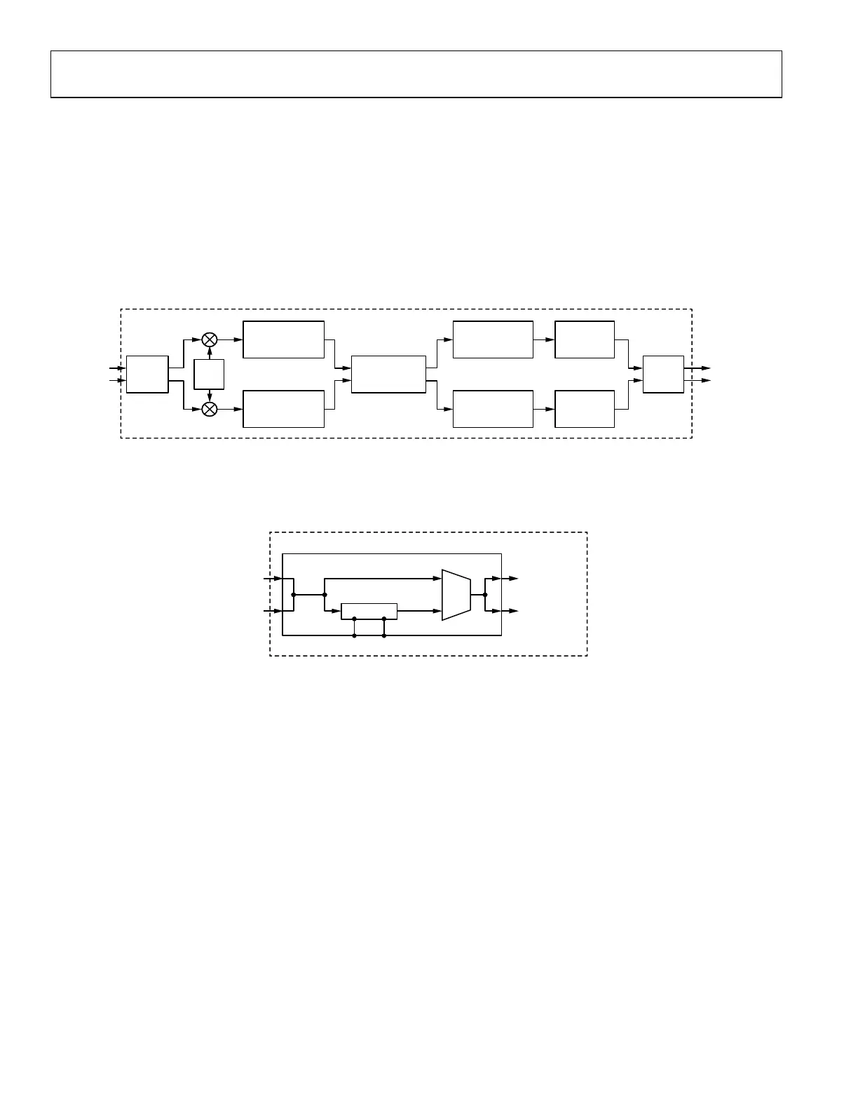
ADRV9001 Rx narrow-band demodulator subsystem, denoted by rxnbdem, is the digital baseband backend partition of ADRV9001 Rx
channel. Note that narrow band, commonly for a wireless communication system, if the channel spacing, also known as channel
bandwidth, is no more than 1 MHz, we call it “Narrowband System”. Otherwise, we call “Wideband System”. Figure 168 illustrates the
rxnbdem subsystem, incorporating signal buffering, carrier frequency offset correction, programmable channel filtering, frequency
discrimination, narrowband programmable pulse shaping, and resampling function. The input of rxnbdem, driven by the RX decimation
filters, is the ZIF digital baseband IQ signal. Programmability exists to bypass each block in the rxnbdem subsystem. The output of
rxnbdem, is directly sent to the RX SSI interface. Depending on the programmed functionality, the output can be Frequency
Deviation(I)-only or IQ.
Figure 168. Functional Diagram of rxnbdem
Signal FIFO
Signal FIFO is to buffer the input IQ data stream, and it is applicable only in the CMOS SSI operation mode. The Signal FIFO depth is
2048. As a result, it can store for more than 85 ms at the sampling rate of 24 kHz
Figure 169. Functional Diagram of Signal FIFO
The Signal FIFO can be disabled or enabled based on the users’ requirement. As the Signal FIFO is disabled, this block is bypassed and
cannot be written or read. As the Signal FIFO is enabled, the writing control and reading control of the Signal FIFO can be manipulated
separately. The FIFO reading clock is configurable, can be 1×, 2×, 4×, or 8× of the FIFO writing clock. For wideband modes, only 1x and
2× are supported and the reading clock rate cannot be above 61.44 MHz.
In the Signal FIFO, as shown in Figure 169 there is an output mux, which has 2 inputs: one input, denoted as “Bypass”, is driven by the
input IQ stream to the FIFO; the other, denoted as “FIFO”, is driven by the output IQ stream from the FIFO. The mux inputs can be
switched on demand to drive the following modules in rxnbdem.
Below is an example explaining how to use the Signal FIFO.
During the signal capturing phase before the wireless data link is established, the mux should be kept at “Bypass”, and the FIFO writing
control is enabled, and the FIFO reading control is disabled. Through the Rx SSI port, the BBIC can keep on detecting the received signal.
Meanwhile, the Signal FIFO keeps on buffering the IQ stream. The FIFO writing overflow may or may not happen. If happen, the FIFO
always stores the latest 2048 IQ data.
As the BBIC detects the wanted Rx frame from the input data stream and estimates the right starting point of the wanted Rx frame,
further the synchronous parameters, the BBIC may switch the mux from “Bypass” to “FIFO”, then enable the reading control of the FIFO,
to process the stored data stream and the following data stream seamlessly.
Carrier Frequency Corrector (CFC)
Carrier Frequency Corrector in rxnbdem is to remove the carrier frequency offset. This module can be bypassed.
RESAMPLER
NB
PROGRAMMABLE
FIR
NB
PROGRAMMABLE
FIR
Rx
PROGRAMMABLE
FIR
Rx
PROGRAMMABLE
FIR
FREQUENCY
DISCRIMINATOR
RESAMPLER
SIGNAL
FIFO
SIN
DDS
COS
DECIMATION
FILTERS
I
Q
I
Q OR Mag
I OR FD
Q OR Mag
I OR FD
Q
I OR FD
Rx SSI
INTERFACE
Q
rxnb_dem
ROUND
I
Q
24159-126
SIGNAL FIFO
FIFO (I+Q)
I+Q
CARRIER
FREQUENCY
CORRECTOR
I
Q
rxnb_dem
DECIMATION
FILTERS
Q
I
BYPASS
FIFO
WRENA
RDENA
24159-127
 Loading...