Preliminary Technical Data UG-1828
Rev. PrC | Page 65 of 338
POWER SAVING FOR LSSI
In TDD mode, the LVDS SSI pads can be powered down/up dynamically based on the Tx_Enable and Rx_Enable level to save power,
three LSSI power down modes are defined for different user’s requirement which are shown in Table 17. API
adi_adrv9001_Ssi_PowerDown_Set is used to set the power down mode for specified channel.
Table 17 LSSI power down mode
LSSI Power Down Mode Description
ADI_ADRV9001_SSI_POWER_DOWN_DISABLED All SSI PADS are powered up in PRIMED
ADI_ADRV9001_SSI_POWER_DOWN_MEDIUM RX_DCLK_OUT and TX_DCLK_OUT SSI pads are
TX_DCLK_IN and all Tx/Rx STROBE and DATA SSI pads are powered down
in PRIMED
ADI_ADRV9001_SSI_POWER_DOWN_HIGH
All SSI pads are powered down in PRIMED
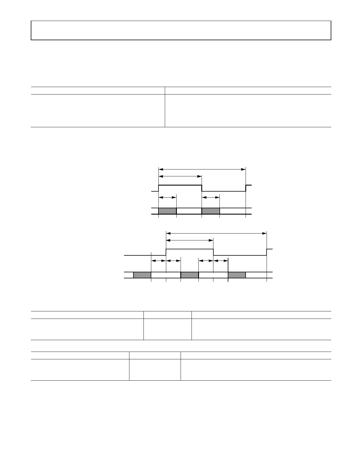
SSI TIMING PARAMETERS
Receive SSI and transmit SSI timing diagram are shown in Figure 54 and Figure 55. The preliminary timing specification for CMOS SSI is
described in Table 18 and the preliminary timing specification for LVDS SSI is described in Table 19.
Figure 54. Receive SSI Timing Diagram
Figure 55. Transmit SSI Timing Diagram
Table 18. CMOS SSI Timing Specification
CMOS SSI Timing Description
DELAY
Clock to strobe/data delay
CMOS Tx t
SETUP
Minimum 2 ns Strobe/data setup to clock
CMOS Tx t
HOLD
Minimum 2 ns Strobe/data hold after clock
Table 19. LVDS SSI Timing Specification
Rx t
DELAY
(Maximum) 200 ps Clock to strobe/data delay
Tx t
SETUP
(Minimum) 250 ps Strobe/data setup to clock
Tx t
HOLD
(Minimum) 550 ps Strobe/data hold after clock
API PROGRAMMING
The ADRV9001 SSI configuration is performed in chip initialization stage and based on the following data structure.
typedef struct adi_adrv9001_SsiConfig
{
adi_adrv9001_SsiType_e ssiType;
DATA
CLOCK PERIOD
DATA
T
DELAY
RX_DCLK_OUT
RX_STROBE/DATA_OUT
T
DELAY
24159-051
DATA
CLOCK PERIOD
DATA
T
SETUP
T
HOLD
TX_DCLK_IN
TX_SROBE/DATA_IN
T
SETUP
T
HOLD
DATA
24159-052
 Loading...