Preliminary Technical Data UG-1828
Rev. PrC | Page 235 of 338
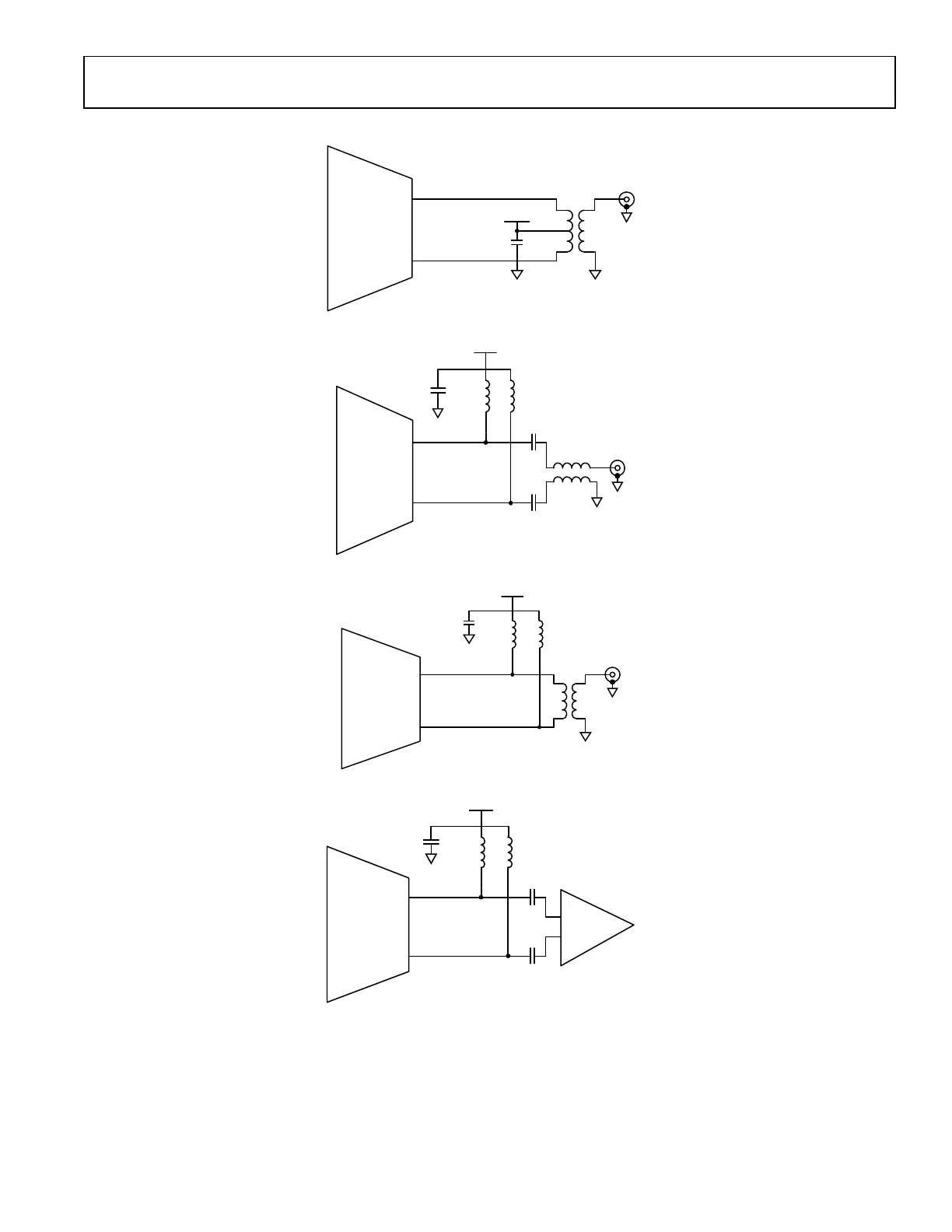
Transmitter Interface Configurations
Figure 220. ADRV9001 RF Transmitter Interface Configuration A
Figure 221. ADRV9001 RF Transmitter Interface Configuration B
Figure 222. ADRV9001 RF Transmitter Interface Configuration C
Figure 223. ADRV9001 RF Transmitter Interface Configuration D
If a Tx balun is selected that requires a set of external dc bias chokes, careful planning is required. It is necessary to find the optimum
compromise between the choke physical size, choke dc resistance (RDCR) and the balun low frequency insertion loss. In commercially
available dc bias chokes, resistance decreases as size increases. However, as choke inductance increases, resistance increases. Therefore, it
is undesirable to use physically small chokes with high inductance as they exhibit the greatest resistance. For example: the voltage drop of
a 500 nH, 0603 choke at 100 mA is roughly 50 mV.
Tx1 OR Tx2
OUTPUT S
T
AGE
1.8V
C
B
24159-170
Tx1–/Tx2–
Tx1+/Tx2+
Tx1 OR Tx2
OUTPUT ST
AGE
C
B
L
C
L
C
1.8V
1.8V
1.8V
C
C
C
C
24159-171
Tx1–/Tx2–
Tx1+/Tx2+
Tx1 OR Tx2
OUTPUT S
TAGE
L
C
L
C
1.8V
1.8V
1.8V
C
B
24159-172
Tx1–/Tx2–
Tx1+/Tx2+
Tx1 OR Tx2
OUTPUT STAGE
C
B
L
C
L
C
1.8V
1.8V
1.8V
C
C
C
C
DRIVER
AMPLIFIER
24159-173
Tx1–/Tx2–
Tx1+/Tx2+
 Loading...