AT90S2313
31
The 16-bit Timer/Counter1 can select clock source from CK, prescaled CK, or an external pin. In addition it can be stopped
as described in the specification for the Timer/Counter1 Control Register - TCCR1B. The different status flags (overflow,
compare match and capture event) and control signals are found in the Timer/Counter Interrupt Flag Register - TIFR. The
interrupt enable/disable settings for Timer/Counter1 are found in the Timer/Counter Interrupt Mask Register - TIMSK.
When Timer/Counter1 is externally clocked, the external signal is synchronized with the oscillator frequency of the CPU. To
assure proper sampling of the external clock, the minimum time between two external clock transitions must be at least one
internal CPU clock period. The external clock signal is sampled on the rising edge of the internal CPU clock.
The 16-bit Timer/Counter1 features both a high resolution and a high accuracy usage with the lower prescaling opportuni-
ties. Similarly, the high prescaling opportunities makes the Timer/Counter1 useful for lower speed functions or exact timing
functions with infrequent actions.
The Timer/Counter1 supports an Output Compare function using the Output Compare Register 1A - OCR1A as the data
source to be compared to the Timer/Counter1 contents. The Output Compare functions include optional clearing of the
counter on compare matches, and actions on the Output Compare pin 1 on compare matches.
Timer/Counter1 can also be used as a 8, 9 or 10-bit Pulse With Modulator. In this mode the counter and the OCR1 register
serve as a glitch-free stand-alone PWM with centered pulses. Refer to page 35 for a detailed description on this function.
The Input Capture function of Timer/Counter1 provides a capture of the Timer/Counter1 contents to the Input Capture Reg-
ister - ICR1, triggered by an external event on the Input Capture Pin - ICP. The actual capture event settings are defined by
the Timer/Counter1 Control Register - TCCR1B. In addition, the Analog Comparator can be set to trigger the Input Capture.
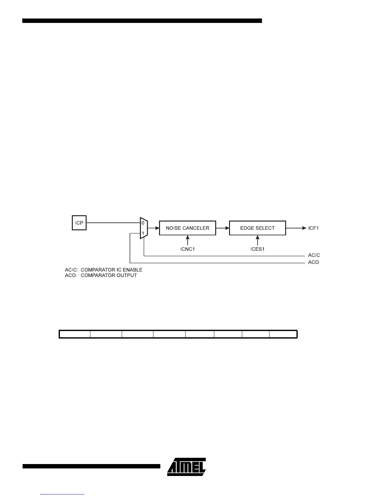
Refer to the section, “Analog Comparator” on page 45, for details on this. The ICP pin logic is shown in Figure 31.
Figure 31. ICP Pin Schematic Diagram
If the noise canceler function is enabled, the actual trigger condition for the capture event is monitored over 4 samples, and
all 4 must be equal to activate the capture flag.
Timer/Counter1 Control Register A - TCCR1A
Bit 7 6 5 4 3 2 1 0
$2F ($4F) COM1A1 COM1A0 - - - - PWM11 PWM10 TCCR1A
Read/Write R/W R/W R R R R R/W R/W
Initial value 0 0 0 0 0 0 0 0