AT90S2313
46
•
Bit 4 - ACI: Analog Comparator Interrupt Flag
This bit is set (one) when a comparator output event triggers the interrupt mode defined by ACIS1 and ACIS0. The Analog
Comparator Interrupt routine is executed if the ACIE bit is set (one) and the I-bit in SREG is set (one). ACI is cleared by
hardware when executing the corresponding interrupt handling vector. Alternatively, ACI is cleared by writing a logic one to
the flag. Observe however, that if another bit in this register is modified using the SBI or CBI instruction, ACI will be cleared
if it has become set before the operation.
•
Bit 3 - ACIE: Analog Comparator Interrupt Enable
When the ACIE bit is set (one) and the I-bit in the Status Register is set (one), the analog comparator interrupt is activated.
When cleared (zero), the interrupt is disabled.
•
Bit 2 - ACIC: Analog Comparator Input Capture Enable
When set (one), this bit enables the Input Capture function in Timer/Counter1 to be triggered by the analog comparator.
The comparator output is in this case directly connected to the Input Capture front-end logic, making the comparator utilize
the noise canceler and edge select features of the Timer/Counter1 Input Capture interrupt. When cleared (zero), no con-
nection between the analog comparator and the Input Capture function is given. To make the comparator trigger the
Timer/Counter1 Input Capture interrupt, the TICIE1 bit in the Timer Interrupt Mask Register (TIMSK) must be set (one).
•
Bits 1,0 - ACIS1, ACIS0: Analog Comparator Interrupt Mode Select
These bits determine which comparator events that trigger the Analog Comparator interrupt. The different settings are
shown in Table 16.
Note: When changing the ACIS1/ACIS0 bits, The Analog Comparator Interrupt must be disabled by clearing its Interrupt Enable bit in
the ACSR register. Otherwise an interrupt can occur when the bits are changed.
I/O-Ports
All AVR ports have true Read-Modify-Write functionality when used as general digital I/O ports. This means that the direc-
tion of one port pin can be changed without unintentionally changing the direction of any other pin with the SBI and CBI
instructions. The same applies for changing drive value (if configured as output) or enabling/disabling of pull-up resistors (if
configured as input).
Port B
Port B is an 8-bit bi-directional I/O port.
Three I/O memory address locations are allocated for the Port B, one each for the Data Register - PORTB, $18 ($38), Data
Direction Register - DDRB, $17($37) and the Port B Input Pins - PINB, $16($36). The Port B Input Pins address is read
only, while the Data Register and the Data Direction Register are read/write.
All port pins have individually selectable pull-up resistors. The Port B output buffers can sink 20mA and thus drive LED dis-
plays directly. When pins PB0 to PB7 are used as inputs and are externally pulled low, they will source current if the
internal pull-up resistors are activated.
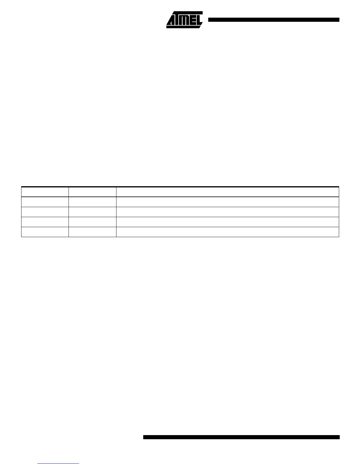
Table 16. ACIS1/ACIS0 Settings
ACIS1 ACIS0 Interrupt Mode
0 0 Comparator Interrupt on Output Toggle
01Reserved
1 0 Comparator Interrupt on Falling Output Edge
1 1 Comparator Interrupt on Rising Output Edge