AT90S2313
47
The Port B pins with alternate functions are shown in the following Table 17:
When the pins are used for the alternate function the DDRB and PORTB register has to be set according to the alternate
function description.
Port B Data Register - PORTB
Port B Data Direction Register - DDRB
Port B Input Pins Address - PINB
The Port B Input Pins address - PINB - is not a register, and this address enables access to the physical value on each Port
B pin. When reading PORTB, the Port B Data Latch is read, and when reading PINB, the logical values present on the pins
are read.
Port B as General Digital I/O
All 8 pins in Port B have equal functionality when used as digital I/O pins.
PBn, General I/O pin: The DDBn bit in the DDRB register selects the direction of this pin, if DDBn is set (one), PBn is con-
figured as an output pin. If DDBn is cleared (zero), PBn is configured as an input pin. If PORTBn is set (one) when the pin
configured as an input pin, the MOS pull up resistor is activated. To switch the pull up resistor off, the PORTBn has to be
cleared (zero) or the pin has to be configured as an output pin The Port B pins are tri-stated when a reset condition
becomes active, even if the clock is not active.
Table 17. Port B Pins Alternate Functions
Port Pin Alternate Functions
PB0 AIN0 (Analog comparator positive input)
PB1 AIN1 (Analog comparator negative input)
PB3 OC1 (Timer/Counter1 Output compare match output)
PB5 MOSI (Data input line for memory downloading)
PB6 MISO (Data output line for memory uploading)
PB7 SCK (Serial clock input)
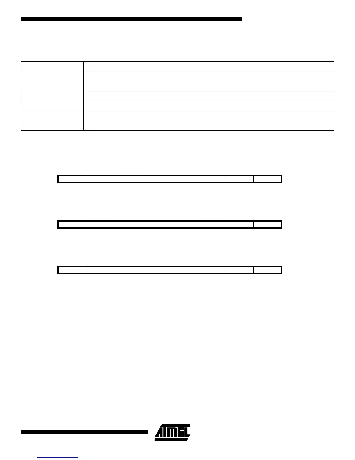
Bit 76543210
$18 ($38) PORTB7 PORTB6 PORTB5 PORTB4 PORTB3 PORTB2 PORTB1 PORTB0 PORTB
Read/Write R/W R/W R/W R/W R/W R/W R/W R/W
Initial value 0 0 0 0 0 0 0 0
Bit 76543210
$17 ($37) DDB7 DDB6 DDB5 DDB4 DDB3 DDB2 DDB1 DDB0 DDRB
Read/Write R/W R/W R/W R/W R/W R/W R/W R/W
Initial value 0 0 0 0 0 0 0 0
Bit 76543210
$16 ($36) PINB7 PINB6 PINB5 PINB4 PINB3 PINB2 PINB1 PINB0 PINB
Read/Write RRRRRRRR
Initial value Hi-Z Hi-Z Hi-Z Hi-Z Hi-Z Hi-Z Hi-Z Hi-Z