17
AT90S2313
0839G–08/01
pose working registers and the I/O space. I/O registers within the address range $00 -
$1F are directly bit-accessible using the SBI and CBI instructions. In these registers, the
value of single bits can be checked by using the SBIS and SBIC instructions. Refer to
the instruction set section for more details. When using the I/O specific commands IN
and OUT, the I/O addresses $00 - $3F must be used. When addressing I/O registers as
SRAM, $20 must be added to this address. All I/O register addresses throughout this
document are shown with the SRAM address in parentheses.
For compatibility with future devices, reserved bits should be written to zero if accessed.
Reserved I/O memory addresses should never be written.
Some of the status flags are cleared by writing a logical “1” to them. Note that the CBI
and SBI instructions will operate on all bits in the I/O register, writing a “1” back into any
flag read as set, thus clearing the flag. The CBI and SBI instructions work with registers
$00 to $1F only.
The I/O and peripherals control registers are explained in the following sections.
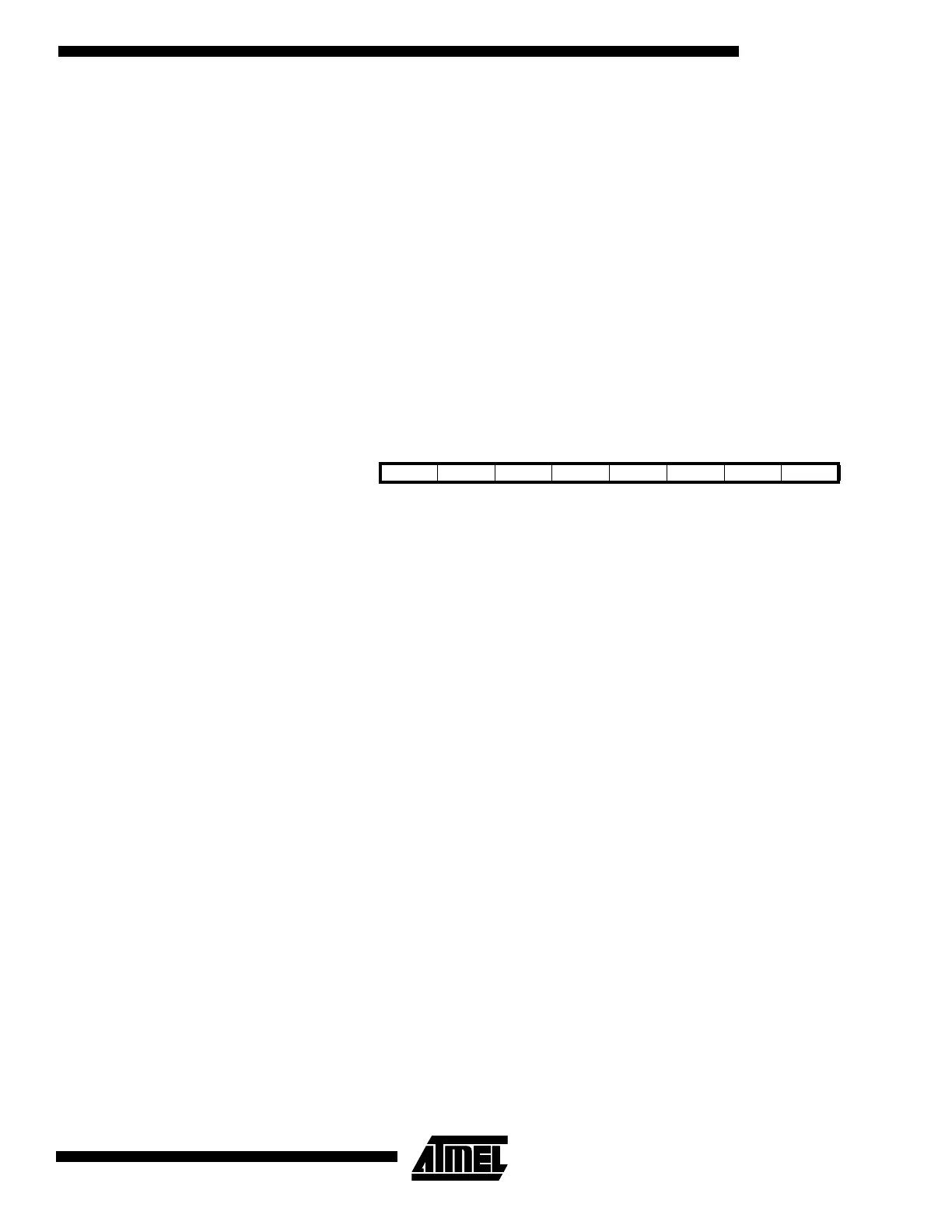
Status Register – SREG The AVR Status Register (SREG) at I/O space location $3F ($5F) is defined as:
• Bit 7 – I: Global Interrupt Enable
The global interrupt enable bit must be set (one) for the interrupts to be enabled. The
individual interrupt enable control is then performed in separate control registers. If the
global interrupt enable bit is cleared (zero), none of the interrupts are enabled indepen-
dent of the individual interrupt enable settings. The I-bit is cleared by hardware after an
interrupt has occurred, and is set by the RETI instruction to enable subsequent
interrupts.
• Bit 6 – T: Bit Copy Storage
The bit copy instructions BLD (Bit LoaD) and BST (Bit STore) use the T-bit as source
and destination for the operated bit. A bit from a register in the register file can be copied
into T by the BST instruction, and a bit in T can be copied into a bit in a register in the
register file by the BLD instruction.
• Bit 5 – H: Half-carry Flag
The half-carry flag H indicates a half-carry in some arithmetic operations. See the
Instruction Set description for detailed information.
• Bit 4 – S: Sign Bit, S = N ⊕ V
The S-bit is always an exclusive or between the negative flag N and the two’s comple-
ment overflow flag V. See the Instruction Set description for detailed information.
• Bit 3 – V: Two’s Complement Overflow Flag
The two’s complement overflow flag V supports two’s complement arithmetics. See the
Instruction Set description for detailed information.
• Bit 2 – N: Negative Flag
The negative flag N indicates a negative result after the different arithmetic and logic
operations. See the Instruction Set description for detailed information.
• Bit 1 – Z: Zero Flag
The zero flag Z indicates a zero result after the different arithmetic and logic operations.
See the Instruction Set description for detailed information.
Bit 76543210
$3F ($5F) I T H S V N Z C SREG
Read/Write R/W R/W R/W R/W R/W R/W R/W R/W
Initial value00000000

 Loading...


