63
AT90S2313
0839G–08/01
Parallel Programming This section describes how to parallel program and verify Flash program memory,
EEPROM data memory, Lock bits and Fuse bits in the AT90S2313.
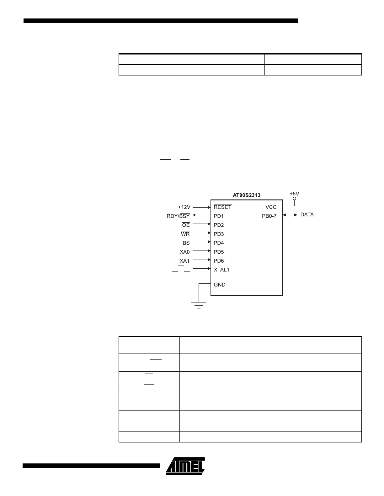
Signal Names In this section, some pins of the AT90S2313 are referenced by signal names describing
their function during parallel programming. Pins not described in the following table are
referenced by pin names. See Figure 49 and Table 23. Pins not described in Table 23
are referenced by pin names.
The XA1/XA0 pins determine the action executed when the XTAL1 pin is given a posi-
tive pulse. The bit coding is shown in Table 24.
When pulsing WR
or OE, the command loaded determines the action executed. The
command is a byte where the different bits are assigned functions as shown in Table 25.
Figure 49. Parallel Programming
.
Table 22. Supply Voltage during Programming
Part Serial Programming Parallel Programming
AT90S2313 2.7 - 6.0V 4.5 - 5.5V
Table 23. Pin Name Mapping
Signal Name in
Programming Mode Pin Name I/O Function
RDY/BSY
PD1 O
0: Device is busy programming, 1: Device is ready
for new command
OE
PD2 I Output Enable (Active low)
WR
PD3 I Write Pulse (Active low)
BS PD4 I
Byte Select (“0” selects low byte, “1” selects high
byte)
XA0 PD5 I XTAL Action Bit 0
XA1 PD6 I XTAL Action Bit 1
DATA PB7-0 I/O Bi-directional Data Bus (Output when OE
is low)

 Loading...


