74
AT90S2313
0839G–08/01
Notes: 1. “Max” means the highest value where the pin is guaranteed to be read as low.
2. “Min” means the lowest value where the pin is guaranteed to be read as high.
3. Although each I/O port can sink more than the test conditions (20 mA at V
CC
= 5V,
10 mA at V
CC
= 3V) under steady state conditions (non-transient), the following must
be observed:
1] The sum of all I
OL
, for all ports, should not exceed 200 mA
2] The sum of all II
OL
, for port D0 - D5 and XTAL2 should not exceed 100 mA.
3] The sum of all I
OL
, for ports B0 - B7 and D6 should not exceed 100 mA.
If I
OL
exceeds the test condition, V
OL
may exceed the related specification. Pins are
not guaranteed to sink current greater than the listed test condition.
4. Although each I/O port can source more than the test conditions (3 mA at V
CC
= 5V,
1.5 mA at V
CC
= 3V) under steady state conditions (non-transient), the following must
be observed:
1] The sum of all I
OH
, for all ports, should not exceed 200 mA
2] The sum of all I
OH
, for port D0 - D5 and XTAL2 should not exceed 100 mA.
3] The sum of all I
OH
, for ports B0 - B7 and D6 should not exceed 100 mA.
If I
OH
exceeds the test condition, V
OH
may exceed the related specification. Pins are
not guaranteed to source current greater than the listed test condition.
5. Minimum V
CC
for power-down is 2V.
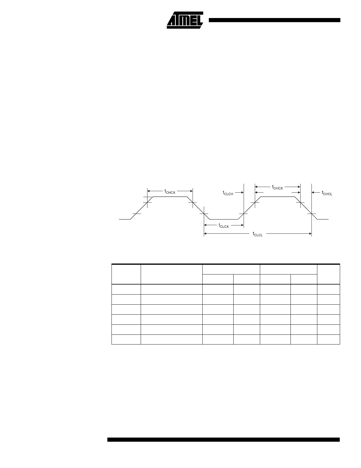
External Clock Drive
Waveforms
Figure 56. External Clock
External Clock Drive
Symbol Parameter
V
CC
= 2.7V to 6.0V V
CC
= 4.0V to 6.0V
UnitsMin Max Min Max
1/t
CLCL
Oscillator Frequency 0 4 0 10.0 MHz
t
CLCL
Clock Period 250.0 100.0 ns
t
CHCX
High Time 100.0 40.0 ns
t
CLCX
Low Time 100.0 40.0 ns
t
CLCH
Rise Time 1.6 0.5 µs
t
CHCL
Fall Time 1.6 0.5 µs
VIL1
VIH1

 Loading...


