PRELIMINARY
Document type: Title: Revision date: Revision:
User's Manual (MUT) Mod. V1729 4 Channel 12 Bit Sampling ADC 22/06/2005 3
NPO: Filename: Number of pages: Page:
00109/04:V1729.MUTx/03 V1729_REV3.DOC 38 26
4.5.6 Straps and resistor network sockets
A certain number of sockets for straps and resistor networks are available on the board.
These are their respective roles:
Reference Role
S1 one utilizes the differential EXT_TRIG differential input (exclusive of S3)
S3 one utilizes the unipolar EXT_TRIG input by Lemo (exclusive of S1)
S2 the BUSY/SYNC_OUT output releases the BUSY signal (exclusive of S4)
S4 the BUSY/SYNC_OUT output releases the SYNC_OUT signal (exclusive of S2)
S5 and S6 address of the board
S7
one utilizes the EXT_CLK input for the main clock (exclusive of S8)
S8
one utilizes the 100MHz oscillator for the main clock (exclusive of S7)
S9
Do not use
S10
choice of the acquisition data bus
S11
normally absent. Prevents the conf_done to rise which then permits not to
validate the configuration of the Altera at power-up.
S12 and
S13
address of the board
J3 adaptation for the EXT_DIFF_TRIG input. Place 100 ohms between the pins 1 and 2
and between the pins 3 and 4
J4 pull-down for the GPIB. Place an 8 resistor network 6.8k with common pin
J5 pull-up for the GPIB. Place an 8 resistor network 3.3k with common pin
J6 pull-down for the GPIB. Place an 8 resistor network 6.8k with common pin
J7 pull-up for the GPIB. Place an 8 resistor network 3.3k with common pin.
Caution : only place these 4 networks once if the boards are linked.
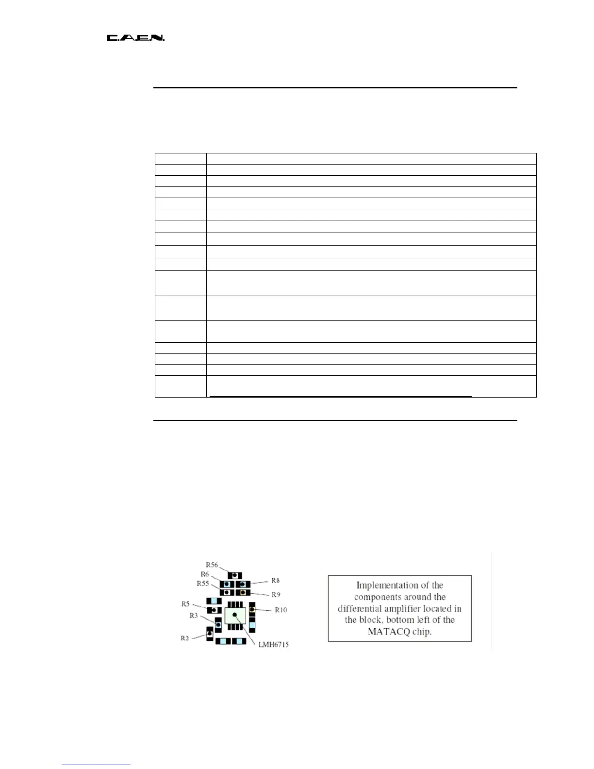
4.5.7 Implementation of differential inputs
The input signals are by default unipolar. In order to use differential inputs, one must
make use of certain free CMS-805 resistor locations located close to the input amplifiers
(LMH6715) and change some others. The equipment map of this zone of the board is
presented below. The already present resistors appear in blue, whereas the free
locations appear in white.
In order to wire a differential input (with both inputs adapted on 50 ohms), one must first
remove the resistors R3, R6 and R8. Then one has to put 84.5 ohms on R2, 0 ohm on
R5 (use the former R3), 121 ohms on R55 and 50 ohms on R56. Finally, R9 (750 ohms)
has to be replaced by 237 ohms and R10 (30.9 ohms) by 10 ohms.
 Loading...