PRELIMINARY
Document type: Title: Revision date: Revision:
User's Manual (MUT) Mod. V1729 4 Channel 12 Bit Sampling ADC 22/06/2005 3
NPO: Filename: Number of pages: Page:
00109/04:V1729.MUTx/03 V1729_REV3.DOC 38 29
(#REG) : ASCII code character corresponding to the sub-address of the register to read
(h0C to read the data stored in the RAM for instance).
* Reading operation of nbyte characters.
In the general case (outside DATA RAM) nbyte =1.
In GPIB, the 16 bits of data converted by the ADC are read in two consecutive bytes in
the order MSByte, LSByte.
Interruption
At the end of the emptying of the data in the RAM, the V1729 board generates a
« Service Request (SRQ)» on the GPIB bus. The board is not compatible with the
PARALLEL or SERIAL POLLING protocols. However the GPIB controller can identify the
SRQ emitor by sequentially scanning the INTERRUPT registers of the different boards. It
is not a source of noise because the acquisition is then already terminated.
Like in VME, the interruption (SRQ) is set back to 0 by any writing at the address of the
INTERRUPT register, or by the START_ACQ command. In the same way, the presence
of waiting data can equally be detected without treating the interruption, but by scanning
the presence of a 1 in the same INTERRUPT register.
Broadcast Mode.
A writing at the address 30 (decimal) permits realization of a writing in all the V1729
boards present on the GPIB bus.
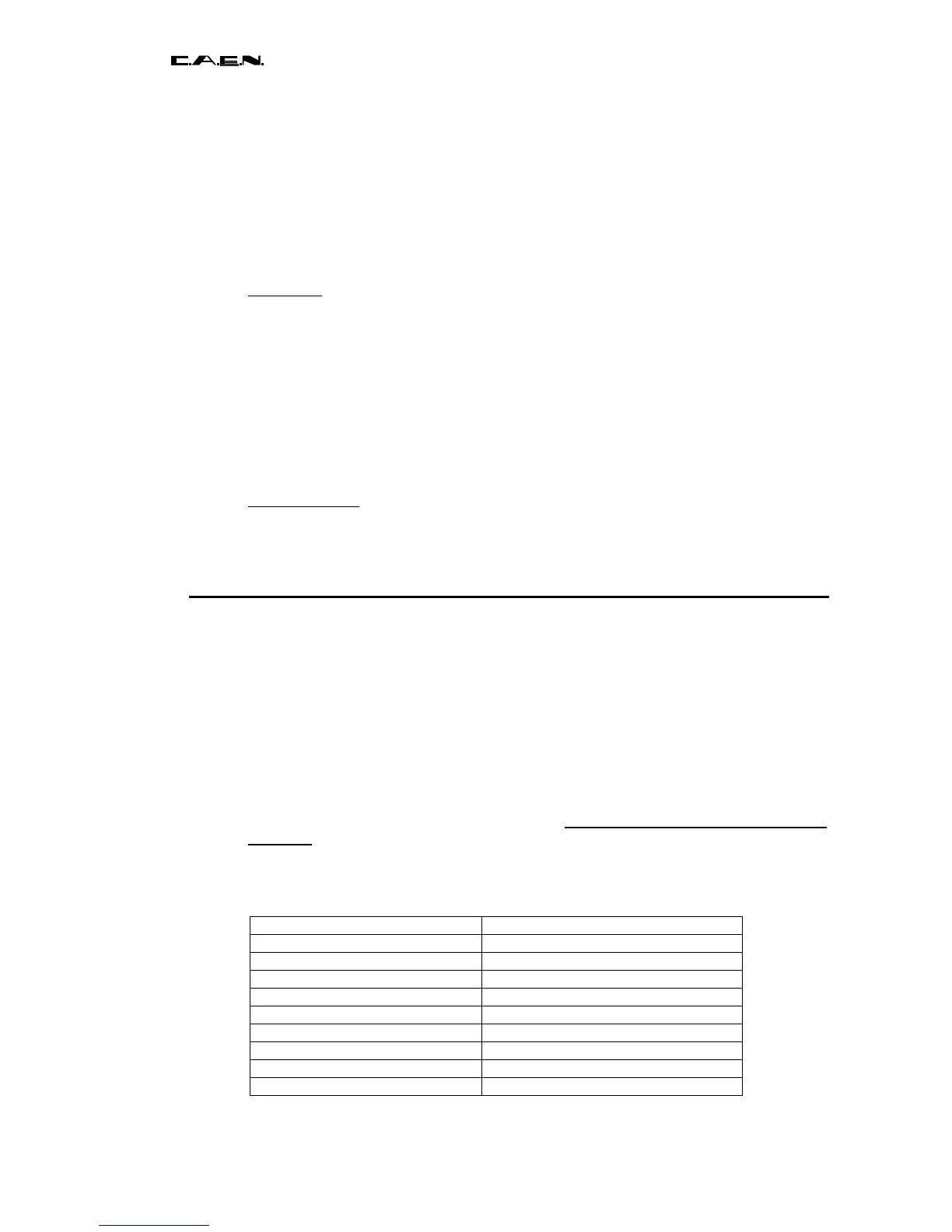
4.7 Reading of the data in the RAM, mapping
During the reading of the MATACQ chips, the data are digitized by the 12-bit ADC then
transferred in the RAM. The sequence order is always the same : one starts by reading
the first cell (upper left-hand) of the matrix, and one finishes with the last one (lower right-
hand), this independently of the position of the trigger and of the stopping point of the
acquisition.
One will therefore have to realign the data in relation to the trigger, which was explained
in 2.5.2. The channels are treated in parallel, and can be masked individually during the
writing in RAM. This implicates that, in the case where NCH channels are validated by
the mask (default value = h0F), the data are organized in 16-bit words by groups of NCH
addresses corresponding to the NCH channels (in the order 3 to 0, minus the masked
channels). The table below clarifies the arrangement of the words in the RAM (10252
words maximum).
The data in the table marked with an asterisk (*) are reserved for expert usage.
RAM internal address (HEX) Type of data
0000 to NCH-1
First sample (*)
NCH to 2*(NCH)-1
Vernier
2*NCH to 3*(NCH)-1
Reset baseline (*)
3*NCH to 4*(NCH)-1
1st cell
4*NCH to 5*(NCH)-1
2
nd
cell
5*NCH to 6*(NCH)-1
3
rd
cell
…
…
2562*NCH to 2563*(NCH)-1
2559th cell
2563*NCH to 2564*(NCH)-1
2560th cell (last cell)