PRELIMINARY
Document type: Title: Revision date: Revision:
User's Manual (MUT) Mod. V1729 4 Channel 12 Bit Sampling ADC 22/06/2005 3
NPO: Filename: Number of pages: Page:
00109/04:V1729.MUTx/03 V1729_REV3.DOC 38 31
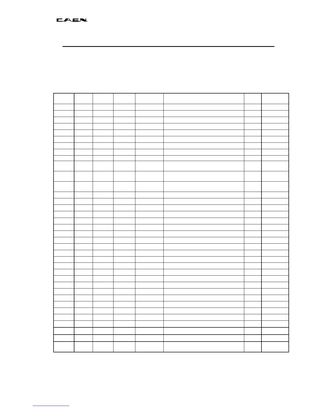
4.8 List of the sub-addresses
The table of the sub-addresses corresponding to the different commands is presented
below. A certain number among them are reserved for expert usage. They are indicated
by the word « RESERVED » in the « NAME » column. They will not be described in this
document and they should not be used. In VME, the sub-addresses are coded over the
bits A8 to A15, the bits A1 to A7 being unused. For more detail on the addressing in VME
or GPIB.
Subadd
(HEX) GPIB VME ACCESS REG or COM. NAME
bits of
data
Default
@ power_on
08 YES YES
W Com RESET BOARD NO
-
09 YES YES
W Com LOAD TRIGGER THRESHOLD DAC NO
-
12 YES YES
W Com RESERVED NO
-
13 YES YES
W Com RESERVED NO
-
14 YES YES
W Com RESERVED NO
-
15 YES YES
W Com RESERVED NO
-
16 YES YES
W Com RESERVED NO
-
17 YES YES
W Com START ACQUISITION NO
-
1C YES YES
W Com SOFTWARE TRIGGER NO
-
0A YES NO
W/R** Reg
TRIGGER THRESHOLD DAC LSB (byte-
>GPIB) 8
0
0B YES NO
W/R** Reg
TRIGGER THRESHOLD DAC MSB
(half byte->GPIB) 4
0
0A NO YES
W/R Reg
TRIGGER THRESHOLD DAC
(word->VME) 12
0
0C YES NO
R Reg RAM DATA MSB + LSB -> GPIB 8
-
0D NO YES
R Reg RAM DATA ->VME 16
-
0E YES YES
W/R Reg RAM_INT_ADD LSB 8
0
0F YES YES
W/R Reg RAM_INT_ADD MSB 8
0
10 YES YES
W/R Reg MAT CTRL REGISTER LSB 8
0
11 YES YES
W/R Reg MAT CTRL REGISTER MSB 8
0
18 YES YES
W/R Reg PRETRIG LSB 8
0
19 YES YES
W/R Reg PRETRIG MSB 8
40
1A YES YES
W/R Reg POSTTRIG LSB 8
64
1B YES YES
W/R Reg POSTTRIG MSB 8
0
1D YES YES
W/R Reg TRIGGER TYPE 5
0
1E YES YES
W/R Reg TRIGGER CHANNEL SOURCE 4
0
20 YES YES
R Reg TRIG_REC 1
-
21 YES YES
W/R Reg FAST READ MODES 2
0
22 YES YES
W/R Reg NB OF COLS TO READ 7
128
23 YES YES
W/R Reg CHANNEL MASKS 4
h0F
24 YES YES
W/R* Reg RESERVED 8
90
30 YES YES
W/R* Reg
POST STOP LATENCY
8
4
31 YES YES
W/R* Reg
POST LATENCY PRETRIG
8
1
80 YES YES
W/R Reg INTERRUPT 1
0
81 YES YES
W/R Reg FP_FREQUENCY 2
1
82 YES YES
R Reg FPGA VERSION 8
-
83 YES YES
W/R Reg EN_VME_IRQ 1
0
FF YES NO
W Reg
NB OF BYTES TO READ IN BLOCK
MODE (GPIB) 24 (3x8)
1
** : no readback of these registers in GPIB.