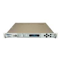
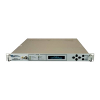
UT-4500 Series C- and Ku-Band Up Converters MN/UT4500.IOM / CD/UT4500.IOM
Table of Contents Revision 3
xiv
A.4.1.3 Manual Configuration and Verification ...................................... A–12
A.4.2 Redundant System Configuration Using the UT-4500 HTTP Interface ... A–14
A.4.3 Offset Adjustment .............................................................................. A–16
A.5 Redundancy Systems – Converter Management ............................... A–16
APPENDIX B. MAINTENANCE AND TROUBLESHOOTING ............ B–1
B.1 Overview .......................................................................................... B–1
B.2 Maintenance Testing ......................................................................... B–2
B.2.1 Sample Test Points ............................................................................... B–2
B.2.2 Troubleshooting ................................................................................... B–3
B.2.3 Converter Faults ................................................................................... B–3
B.2.3.1 Prime Power ................................................................................. B–3
B.2.3.2 DC Power Supply Module ............................................................. B–3
B.2.3.3 RF Converter Module ................................................................... B–4
B.2.3.4 Synthesizer Sum Loop Module ..................................................... B–4
B.2.3.5 Synthesizer Fine Step Module ...................................................... B–4
B.2.3.6 Reference Oscillator Module ........................................................ B–4
B.2.3.7 Temperature Fault ........................................................................ B–5
B.2.4 Removable “Personality” Modules ...................................................... B–5
B.3 Spares ............................................................................................... B–6
B.4 Redundancy Systems – Converter Management ................................. B–6
B.4.1 Remove a Faulted Converter ................................................................ B–6
B.4.2 Install a Replacement Converter ......................................................... B–7
TABLES
Table 4-1. ‘Ethernet’ M&C Interface Connector Pinout .................................... 4–13
Table 4-2. ‘J1 | COM1’ 2-Wire EIA-485 Pinout .................................................. 4–13
Table 4-3. ‘J1 | COM1’ 4-Wire EIA-485 Pinout .................................................. 4–13
Table 4-4. ‘J1 | COM1’ EIA-232C Pinout ............................................................ 4–13
Table 4-5. ‘P1 | RELAY’ Pinout ........................................................................... 4–14
Table 4-6. ‘J3 | HSB’ Data Interface Pinout ....................................................... 4–17