CY7C68013
Document #: 38-08012 Rev. *A Page 27 of 48
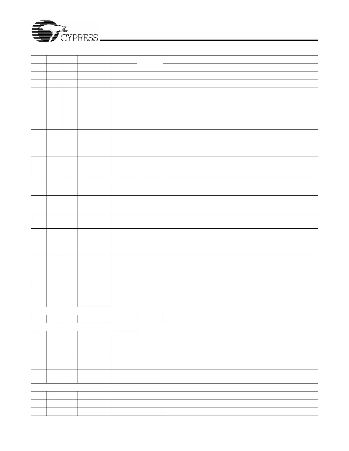
66 51 CTL3 Output H CTL3 is a GPIF control output.
67 52 CTL4 Output H CTL4 is a GPIF control output.
98 76 CTL5 Output H CTL5 is a GPIF control output.
32 26 20 IFCLK I/O/Z Z Interface Clock, used for synchronously clocking data into or out of
the slave FIFOs. IFCLK also serves as a timing reference for all slave
FIFO control signals and GPIF. When internal clocking,
IFCONFIG.7 = 1, is used the IFCLK pin can be configured to output
30/48 MHz by bits IFCONFIG.5 and IFCONFIG.6. IFCLK may be
inverted, whether internally or externally sourced, by setting the bit
IFCONFIG.4 =1.
28 22 INT4 Input N/A INT4 is the 8051 INT4 interrupt request input signal. The INT4 pin is
edge-sensitive, active HIGH.
106 84 INT5# Input N/A INT5# is the 8051 INT5 interrupt request input signal. The INT5 pin
is edge-sensitive, active LOW.
31 25 T2 Input N/A T2 is the active-HIGH T2 input signal to 8051 Timer2, which provides
the input to Timer2 when C/T2 = 1. When C/T2 = 0, Timer2 does not
use this pin.
30 24 T1 Input N/A T1 is the active-HIGH T1 signal for 8051 Timer1, which provides the
input to Timer1 when C/T1 is 1. When C/T1 is 0, Timer1 does not use
this bit.
29 23 T0 Input N/A T0 is the active-HIGH T0 signal for 8051 Timer0, which provides the
input to Timer0 when C/T0 is 1. When C/T0 is 0, Timer0 does not use
this bit.
53 43 RXD1 Input N/A RXD1is an active-HIGH input signal for 8051 UART1, which provides
data to the UART in all modes.
52 42 TXD1 Output H TXD1is an active-HIGH output pin from 8051 UART1, which provides
the output clock in sync mode, and the output data in async mode.
51 41 RXD0 Input N/A RXD0 is the active-HIGH RXD0 input to 8051 UART0, which provides
data to the UART in all modes.
50 40 TXD0 Output H TXD0 is the active-HIGH TXD0 output from 8051 UART0, which pro-
vides the output clock in sync mode, and the output data in async
mode.
42 CS# Output H CS# is the active-LOW chip select for external memory.
41 32 WR# Output H WR# is the active-LOW write strobe output for external memory.
40 31 RD# Output H RD# is the active-LOW read strobe output for external memory.
38 OE# Output H OE# is the active-LOW output enable for external memory.
33 27 21 Reserved Input N/A Reserved. Connect to ground.
101 79 51 WAKEUP Input N/A USB Wakeup. If the 8051 is in suspend, asserting this pin starts up
the oscillator and interrupts the 8051 to allow it to exit the suspend
mode. Holding WAKEUP asserted inhibits the EZ-USB chip from sus-
pending. This pin has programmable polarity (WAKEUP.4).
36 29 22 SCL OD Z Clock for the I
2
C-compatible interface. Connect to V
CC
with a 2.2K
resistor, even if no I
2
C-compatible peripheral is attached.
37 30 23 SDA OD Z Data for I
2
C-compatible interface. Connect to V
CC
with a 2.2K re-
sistor, even if no I
2
C-compatible peripheral is attached.
216V
CC
Power N/A V
CC
. Connect to 3.3V power source.
17 16 14 V
CC
Power N/A V
CC
. Connect to 3.3V power source.
26 20 18 V
CC
Power N/A V
CC
. Connect to 3.3V power source.
Table 4-1. FX2 Pin Descriptions
[5]
(continued)
128 100 56 Name Type Default Description
 Loading...


