CY7C68013
Document #: 38-08012 Rev. *A Page 37 of 48
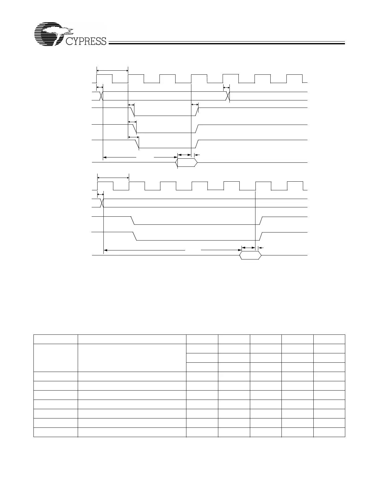
9.3 Data Memory Read
Note:
11. t
ACC2
and t
ACC3
are computed from the above parameters as follows:
t
ACC2
(24 MHz) = 3*t
CL
– t
AV
–t
DSU
= 106 ns
t
ACC2
(48 MHz) = 3*t
CL
– t
AV
– t
DSU
= 43 ns
t
ACC3
(24 MHz) = 5*t
CL
– t
AV
–t
DSU
= 190 ns
t
ACC3
(48 MHz) = 5*t
CL
– t
AV
– t
DSU
= 86 ns.
Table 9-2. Data Memory Read Parameters
Parameter Description Min. Typ. Max. Unit Notes
t
CL
1/CLKOUT Frequency 20.83 ns 48 MHz
41.66 ns 24 MHz
83.2 ns 12 MHz
t
AV
Delay from Clock to Valid Address 10.7 ns
t
STBL
Clock to RD LOW 11 ns
t
STBH
Clock to RD HIGH 11 ns
t
SCSL
Clock to CS LOW 13 ns
t
SOEL
Clock to OE LOW 11.1 ns
t
DSU
Data Set-up to Clock 9.6 ns
t
DH
Data Hold Time 0 ns
data in
t
CL
A[15..0]
t
AV
t
AV
RD#
t
STBL
t
STBH
t
DH
D[7..0]
data in
t
ACC1
[11]
t
DSU
Stretch = 0
Stretch = 1
t
CL
A[15..0]
t
AV
RD#
t
DH
D[7..0]
t
ACC1
[11]
t
DSU
CS#
CS#
t
SCSL
OE#
t
SOEL
Figure 9-2. Data Memory Read Timing Diagram
CLKOUT
[9]
CLKOUT
[9]